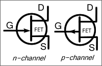
It's the direction of the arrow that tells you:
N-Channel

P-Channel

The arrow points from P to N (like a diode) so you can tell which is which channel wise. For example in the top diagram, the arrow points to the channel, so the channel is N-type. In the bottom diagram it points away, so the channel is P-type (i.e. from P to N)
To clarify, this also applies to the symbol that has the gate connection drawn in the middle:

As far as I am aware, this should be used only when the source/drain are interchangeable, but is often used in error (many JFETs are not symmetrical so cannot be used either way round)
If a JFET is symmetrical, it can be used either way round and work just the same. In this case I think it is just convention to call one terminal source and the other drain even though it doesn't matter in practice.
However, some JFETs are designed so the channel is not the same thickness all the way along, and gate-drain capacitance differs from gate-source capacitance. This will matter little for many applications and the device can still be used either way round, but may be important in some (e.g. high frequency) applications.
I couldn't find any good references that go into detail on the subject quickly but Google for "Asymmetrical JFET" and have a read of the various patents. Also "Art of electronics" has a brief mention of this.


