2
\$\begingroup\$

I am using LTspice to simulate a buck converter, but I am not getting the expected output voltage and I don't understand why.

The specification is simple: I need to get an output voltage which is half of the input one. This is the circuit I am using in the simulation:

enter image description here

I am using a 100kHz PWM, with a duty rate of 50%, and the value of the inductance was chosen using the lower bound to keep the circuit in CCM (using the formula L > D.(Vin-Vout)/(f.0,2.i), where D is the duty ratio, f is the frequency and I am supposing a 20% oscillation in the load current i).

The result that I obtain from the simulation is:

enter image description here

I don't get the 6.5V that are expected at the output. Is there any conceptual mistake here?

Thank you

\$\endgroup\$

4 Answers 4

4
\$\begingroup\$

If all you want is to simulate, then a behavioural approach might be more handy than using real curcuit elements, such as a MOS (which, as I see, and as the other answers say, you have trouble setting it right). Instead, you can use the voltage controlled switch.

The control voltage you're using for that MOS is using a zero rise/fall time, which can't be physically true (no instant rise/fall in nature), so LTspice sets it, by default, to 10% of the Ton. In this case, for Ton=5\$\mu\$s, Trise=Tfall=1\$\mu\$s, which not only gives you an awful transition time, but also extends the value of Ton, from 50% Trise to 50% Tfall, to Ton+(Trise+Tfall)/2=6\$\mu\$s.

Your other values, for LC filter, for example, are awfully chosen: 1H and 10nF? How did you calculate those? I'll skip the load, maybe you intended to see the open load output? Somehow I doubt it.

If you're using the default diode, it would help setting its parameters epsilon and revelsilon, which control the knee-region to be a simple quadratic approximation, thus avoiding the sharp transitions that can cause the solver to yield timestep too small errors due to the possible discontinuity that results in a sharp derivative around that point. Or, you can keep things simple and use the default, quasi-real model by simply setting .model d d Cjo=1p, which only adds a capacitance to the junction in order to improve comvergence, while discarding the ideal model.

Also, using startup and uic, both, is not redundant, but not recommended, either (unless there are strict specifications, are there?). In your case, you're starting a switching application, so neither are needed.

Here's a reworked version of what you need, with some recalculated values for a 6.5V@1A output:
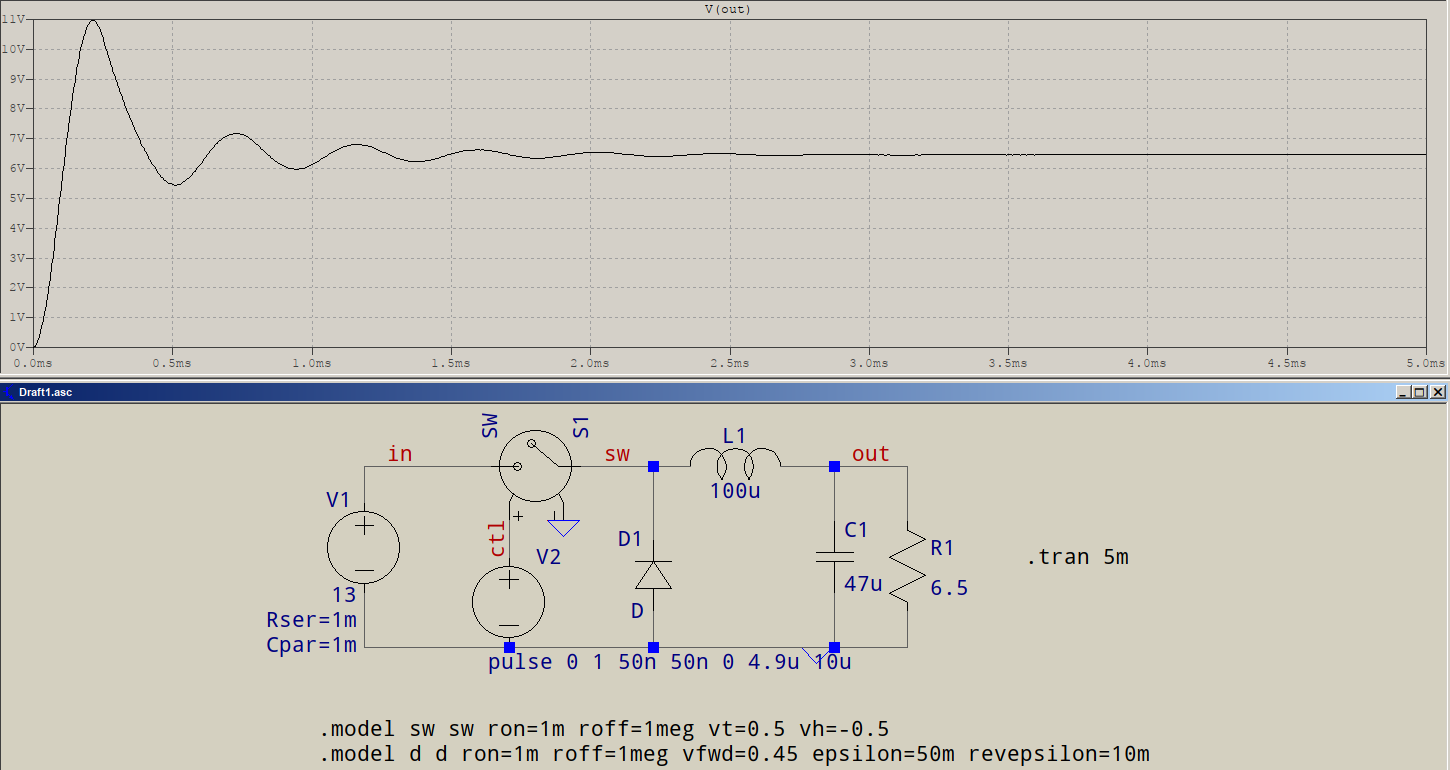
buck

I fully agree with @Dave Tweed, too often people rush to blame the tool rather than the user.


Here's what a quasi-real setup would be:

pmos

Note the PMOS (usually when in high side), driven by a signal that's between GND and 13V (or close, some losses simulated) -- as the other answers have suggested --, and some parasitics. Instead of V2 there's usually some sort of control, voltage- or current-mode, that's a different question, but one that you should be able to find already answered.

\$\endgroup\$
2
  • 1
    \$\begingroup\$ Thank you! But how do I go from this behavioural approach to a real circuit using an NMOS transistor? Are there other subcircuits that need to be designed in order to get this result using a circuit replacing the switch with a transistor? \$\endgroup\$ Commented May 5, 2018 at 16:43
  • 2
    \$\begingroup\$ @ViníciusLopesSimões See the updated answer. Note that the parts used here are in no way representative to a real design -- that's up to you to determine. I merely used them as a reference. \$\endgroup\$ Commented May 5, 2018 at 17:19
4
\$\begingroup\$

Yes. You are using a N-channel MOSFET as your switching element, and driving it with a signal that only goes to +5V.

The MOSFET is operating as a source-follower when it is on, and the output voltage can only rise as far as Vg - Vth, which in this case is only about 1.6 V

Either use a P-channel MOSFET, driven with a gate signal that is negative with respect to its source voltage (the supply voltage), or use a proper N-channel MOSFET driver that can drive the gate above the input voltage.

Note that if you had simply plotted the voltage across the diode, this would have been pretty obvious. I can never understand why people use simulators, and then don't take advantage of all the information they have to offer...

\$\endgroup\$
1
  • 3
    \$\begingroup\$ +1 for the rant about people not taking advantage of the simulation tools. \$\endgroup\$
    – Andy aka
    Commented May 3, 2018 at 21:24
4
\$\begingroup\$

On top of what Dave said, instead of using generic models, try assigning a real MOS and a real diode by right clicking on each component and then on "Pick New MOSFET" and "Pick New Diode". This might allow you to obtain a better result. You still won't get the result you expect because of the losses. You will probably need to modify the duty cycle a little bit.

\$\endgroup\$
3
\$\begingroup\$

I suspect you don’t know the rule of thumb that Vgs must be greater than 2.5 x Vt to get a reasonable RdsOn.

It may be more for 2~4V threshold devices and less for Vt<1V. Where Vt == gs(th). Worst case

\$\endgroup\$

Your Answer

By clicking “Post Your Answer”, you agree to our terms of service and acknowledge you have read our privacy policy.

Not the answer you're looking for? Browse other questions tagged or ask your own question.