2
\$\begingroup\$

The recommended power schematics for Atmel's AT32UC3C (figure 6-1) shows the use of 2 decoupling capacitors from the power supply to the digital circuitry, CIN1 and CIN2. These are meant to decouple VDDIO1, VDDIO2, VDDIO3, and VDDIN_5. However, the pin layout of the chip has these pins on different sides of the IC, each with their individual grounds.

The IC is 16mm*16mm so it seems to me that the traces connecting all the pins to a common decoupling capacitor set might get quite long (somewhere I found a recommendation that decoupling capacitors should be within 1/2" of the pins).

Should I duplicate CIN1/CIN2 for each VDDIOx/GNDIOx combination? Why or why not? If not, which pins should I place the decoupling capacitors closest to, if it even matters?

\$\endgroup\$

3 Answers 3

6
\$\begingroup\$

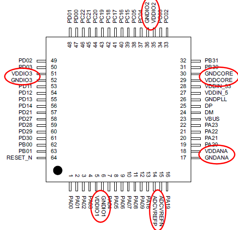
The designers did a perfect job in the pin assignment:

enter image description here

Each of the power pins is right next to a ground pin; you can't get better than that! All you have to do is place the caps on each of the pin pairs, as close as possible to the pins.

\$\endgroup\$
5
  • \$\begingroup\$ So I should be decoupling each source/ground pair? It makes sense conceptually, but that seems at odds with what some of the other posts have said and seems to contradict what I can make of the datasheet figure 6-1. In the datasheet, the analog circuit is decoupled from the digital circuit and that's it. \$\endgroup\$ Commented Aug 11, 2012 at 0:33
  • \$\begingroup\$ @hello - that figure just shows what pins should be connected to which power supply. It's not a complete schematic. They presume that the designer will take the usual decoupling precautions. Matt is not correct on this. Why do you think they are placed like this: VDDIO3 next to a GNDIO3 etc.? \$\endgroup\$
    – stevenvh
    Commented Aug 11, 2012 at 0:39
  • 1
    \$\begingroup\$ Ok, so after some more reading about decoupling capacitors they're only required if operating at "high" frequencies (as determined by power supply current fluctuations and a few other factors). So long story short, while they may not be required probably better to have them anyways. \$\endgroup\$ Commented Aug 11, 2012 at 1:00
  • \$\begingroup\$ The point is that you want the decoupling capacity to be as close as possible to the source... in this case, that's the pins going into the molded body of the IC. In layman terms, this gives you the best decoupling. While all the VDDIO pins might not be splitting up current requirements equally... it's easier and simpler to decouple each pair individually and have that added insurance. (someone feel free to correct me if I'm wrong) \$\endgroup\$ Commented Aug 11, 2012 at 1:21
  • \$\begingroup\$ @helloworld922 - yes, the need (or lack of need) for individual decoupling capacitors depends on the switching loads, in this case mostly of the I/Os. We don't have enough information to definitively answer that. Presence of low-impedance power/ground planes would also impact the requirement - you are more likely to need individual decoupling on a two layer board with poor power routing than on a 4 or more layer board where you can dedicate planes. An SOC where most operations are on chip shouldn't be too demanding on the I/O supplies, but beware any high speed or wide external interfaces. \$\endgroup\$ Commented Aug 11, 2012 at 1:58
4
\$\begingroup\$

Decoupling capacitors should be as close to the pin as possible. Check out Table 40-19 in that datasheet. It outlines the actual decoupling requirements. The way I read the datasheet, I would get the decoupling capacitors right up next to VDDIN_5. That seems to be the power pin that powers the entire IC. You shouldn't need to decouple the VDDIOx pins separately.

\$\endgroup\$
1
  • 1
    \$\begingroup\$ The GNDIO pins right next to each VDDIO are to connect a decoupling capacitor to. \$\endgroup\$
    – stevenvh
    Commented Aug 20, 2012 at 18:37
4
\$\begingroup\$

VDDIN_5 supplied the internal 3V3 regulator and then the 1V8 regulator for the core.

The VDDIO pins supply VDD to the IO pins. Those caps are important to stop switching noise from the IOs getting into the rest of your circuit. If you are not using any of the IO's connected to a particular pin you could possibly leave off the cap.

We just put 100n close to the VDDIOs and have had no problems. There are GND pins right next to them.

You need to connect all the GND pins to each other externally and likewise with the VDD pins

\$\endgroup\$

Your Answer

By clicking “Post Your Answer”, you agree to our terms of service and acknowledge you have read our privacy policy.

Not the answer you're looking for? Browse other questions tagged or ask your own question.