0
\$\begingroup\$

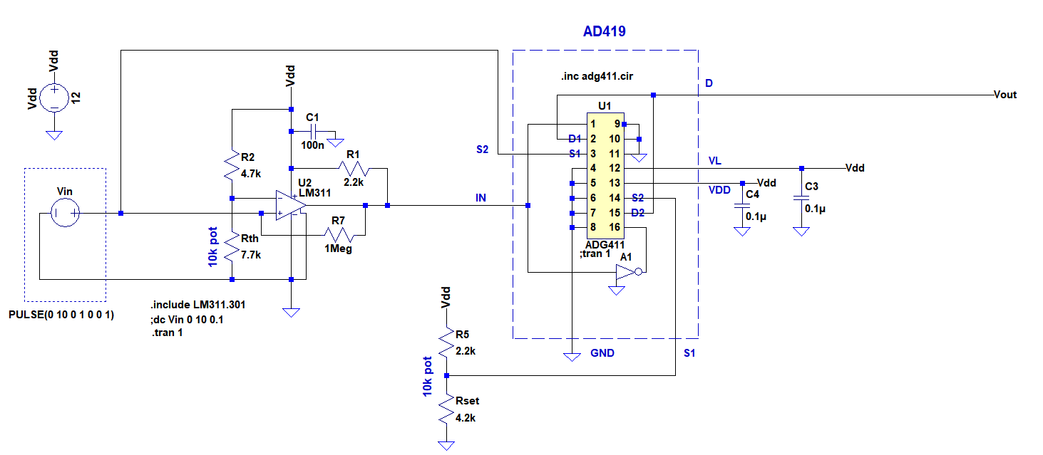
This is directly related to my previous question, so it requires to first have a look at that. And the below LTspice implementation is based on Andy Aka's answer. The following circuit works in LTspice. But I have some observations and questions before I solder it on a board.

First of all, I would like to mention that since I couldn't find the SPICE model for DG419 (analog SPDT switch IC), I made an ADG419 from an ADG411. I read they use the same components inside. So I just needed to invert one input and tie two outputs and it works and mimics ADG419.

A 10k potentiometer Rth will set the threshold voltage, and another 10k pot Rset will set the pre-set voltage Vset.
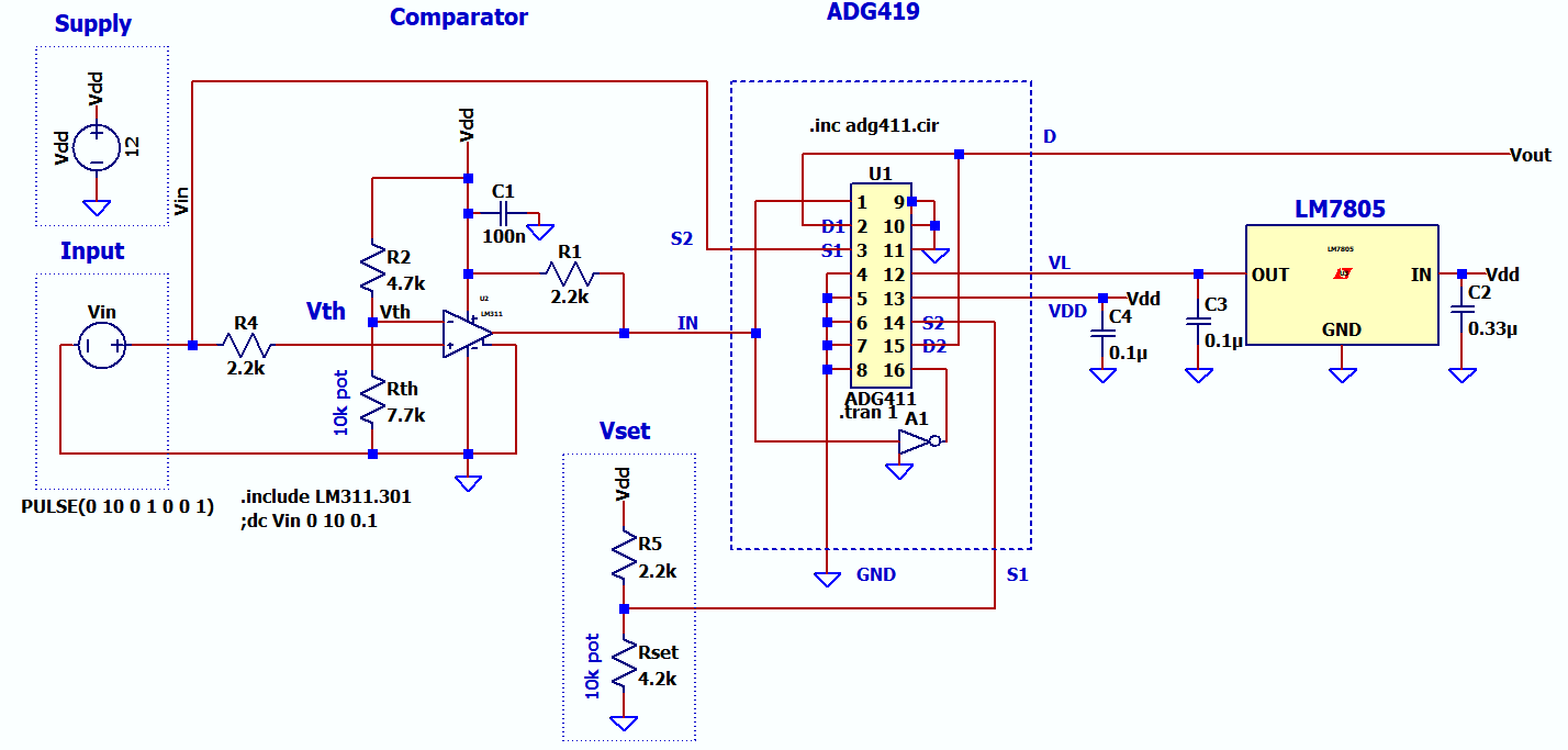
zero through ten volt sweep (left-click to enlarge the schematics)

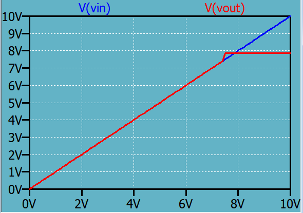
Here is the 0-10V DC sweep:

transient plot

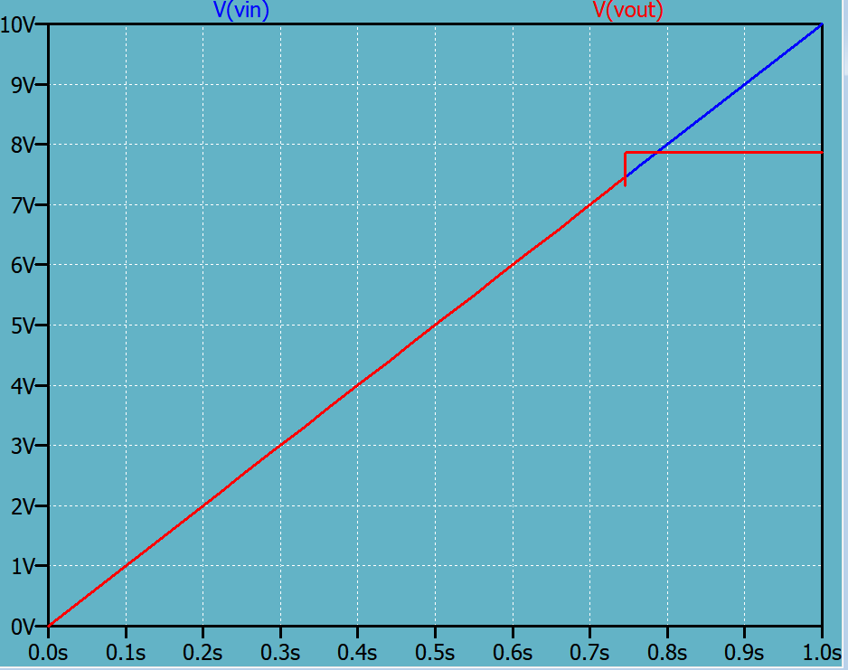
And here is a transient analysis plot for 0-10V in 1 sec (notice the glitch during the comparator action):

glitch

And here is the change at Vth during the comparator action (voltage at the node between R2 and Rth):

threshold change

My questions are:

  1. Is interfacing the comparator LM311 output to the ADG419's input fine this way as in the schematics?
  2. Is that glitch the product of the change in Vth in comparator action? And can that be mitigated? (I don't see the glitch in DC sweep)
  3. Is there any fundamental problem with this circuit or resistor values? Or any peculiarity. For example I'm not sure whether R4 is necessary? (I found it from a circuit I made years ago so I don't remember why it is there.)

Edit:

enter image description here

\$\endgroup\$
6
  • \$\begingroup\$ I don't think you need to have a 5 volt regulator powering the chip. According to the data sheet, the logic supply can run at Vdd and then you don't need to worry about current limiting the comparator output into the control pin. As it stands it will cause problems because of this and may result in the problem you are seeing. \$\endgroup\$
    – Andy aka
    Commented May 30, 2018 at 8:53
  • \$\begingroup\$ Thanks, please see my update: i.sstatic.net/QSqu9.png I removed R4. I supplied logic supply directly from Vdd as you say, I then directly coupled the LM311 output to the control input(so I dont use voltage divider to obtain 5V); and I added 1Meg positive feedback. Is it better than the previous= \$\endgroup\$
    – user16307
    Commented May 30, 2018 at 9:50
  • \$\begingroup\$ Im not sure if the R4 resistor makes sense there, I have used it before for another circuit but I dont remember why for that case. \$\endgroup\$
    – user16307
    Commented May 30, 2018 at 9:55
  • \$\begingroup\$ "Is it better than the previous" - it's only better if the response looks better! \$\endgroup\$
    – Andy aka
    Commented May 30, 2018 at 10:06
  • \$\begingroup\$ Glitch got a bit smaller. the current drawn by control pin is nA level. So better in a way that I dont have to use 2 more resistors and a voltage divider. \$\endgroup\$
    – user16307
    Commented May 30, 2018 at 10:17

2 Answers 2

1
\$\begingroup\$

1-) Is interfacing the comparator LM311 output to the ADG419's input fine this way as in the schematics?

Nope. Pay more attention to the ADG411 data sheet. Pin 5 is the logic supply voltage, and should be 5 volts, not ground. Then the LM311 output should swing from zero to about 5 volts. You can do this with a voltage divider to +12, or tie your pullup to your 5 volt supply. Likewise, your inverter will need to be powered by 5 volts.

An additional issue is your lack of hysteresis on the LM311 - a real circuit may not switch smoothly as you pass through the transition point.

2-) Is that glitch the product of the change in Vth in comparator action? And can that be mitigated?(I don't see the glitch in DC sweep)

Nope, it's due to the fact that your switching point level is less than the level you use to provide the clamped output. 4.7k/7.7k does not give the same level as 2.2k/4.2k.

3-) Is there any fundamental problem with this circuit or resistor values? Or any peculiarity. For example I'm not sure whether R4 necessary?(I found it from a circuit I made years ago so I don't remember why it is there)

It ought to work, although as stated in 1) you should consider adding some positive feedback (even a 1M will do nicely).

\$\endgroup\$
2
  • \$\begingroup\$ Data-sheet says both ADG419 and ADG411 logic supply can run ad Vdd. Pin 5 is the logic supply voltage for ADG419, but in my schematics I'm mimicking ADG419 by using an ADG411 whose logic supply pin is 12. When I removed R4 glitch disappeared. DO i really need a resistor R4 there? And these chips can take control input up to supply voltage. \$\endgroup\$
    – user16307
    Commented May 30, 2018 at 9:45
  • \$\begingroup\$ Here is my update: i.sstatic.net/QSqu9.png \$\endgroup\$
    – user16307
    Commented May 30, 2018 at 9:51
0
\$\begingroup\$

Your switch is rated for 30mA of continuous current, thus I suggest that it might not be the best way to drive a 7805, depending on what you're trying to power.

\$\endgroup\$
4
  • \$\begingroup\$ That is for the VL 5V logic input pin for ADG419. Is 30mA too much? \$\endgroup\$
    – user16307
    Commented May 29, 2018 at 19:55
  • \$\begingroup\$ @WhatRoughBeast VL is not input it is already supplied by 5V regulator \$\endgroup\$
    – user16307
    Commented May 29, 2018 at 20:00
  • \$\begingroup\$ I will add datasheet \$\endgroup\$
    – user16307
    Commented May 29, 2018 at 20:00
  • \$\begingroup\$ @user16307 Oops. Sorry. \$\endgroup\$ Commented May 29, 2018 at 21:05

Your Answer

By clicking “Post Your Answer”, you agree to our terms of service and acknowledge you have read our privacy policy.

Not the answer you're looking for? Browse other questions tagged or ask your own question.