4
\$\begingroup\$

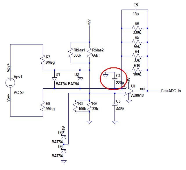
I inherited a opamp measurement circuit that is supposed to be able to measure differential voltages of up to 1000 V with a bandwidth of 1 MHz and a protective impedance between the HV and SELV side. The 0-1000 V on the primary side are converted to 1.5 V - 3.5 V on the secondary. It is basically a differential amplifier with 9 megaohm resistors so that no lethal currents can flow.

The 1.5 V offset is applied via the (66 kohm//330 kohm) to (33 kohm//100 kohm) voltage divider and to avoid troubles caused by the common mode the same impedance is used in the feedback path.
To prevent troubles with the input capacitance of the opamp or the capacitance of the diodes 220 pF capacitors are used to add a defined capacity (again in both paths because of possible common mode problems otherwise).
The problems with these capacitors is that they would limit the bandwidth to 40 kHz and add a pole at around 1 MHz which they circumvented with a 15 pF in the feedback.
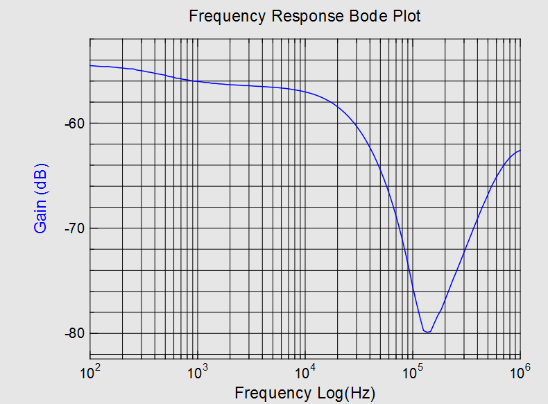
When I tried making their circuit (which worked for them, they used the same opamps and very similar caps) the frequency response of mine always has a notch at around 200 kHz which I can't explain myself.

Does anyone have any idea which parasitic or stupidity of mine could cause such a deviation from the simulated frequency response.

Schematic: Schematic Simulated frequency response: Simulated frequency response Measured frequency response: Measured frequency response
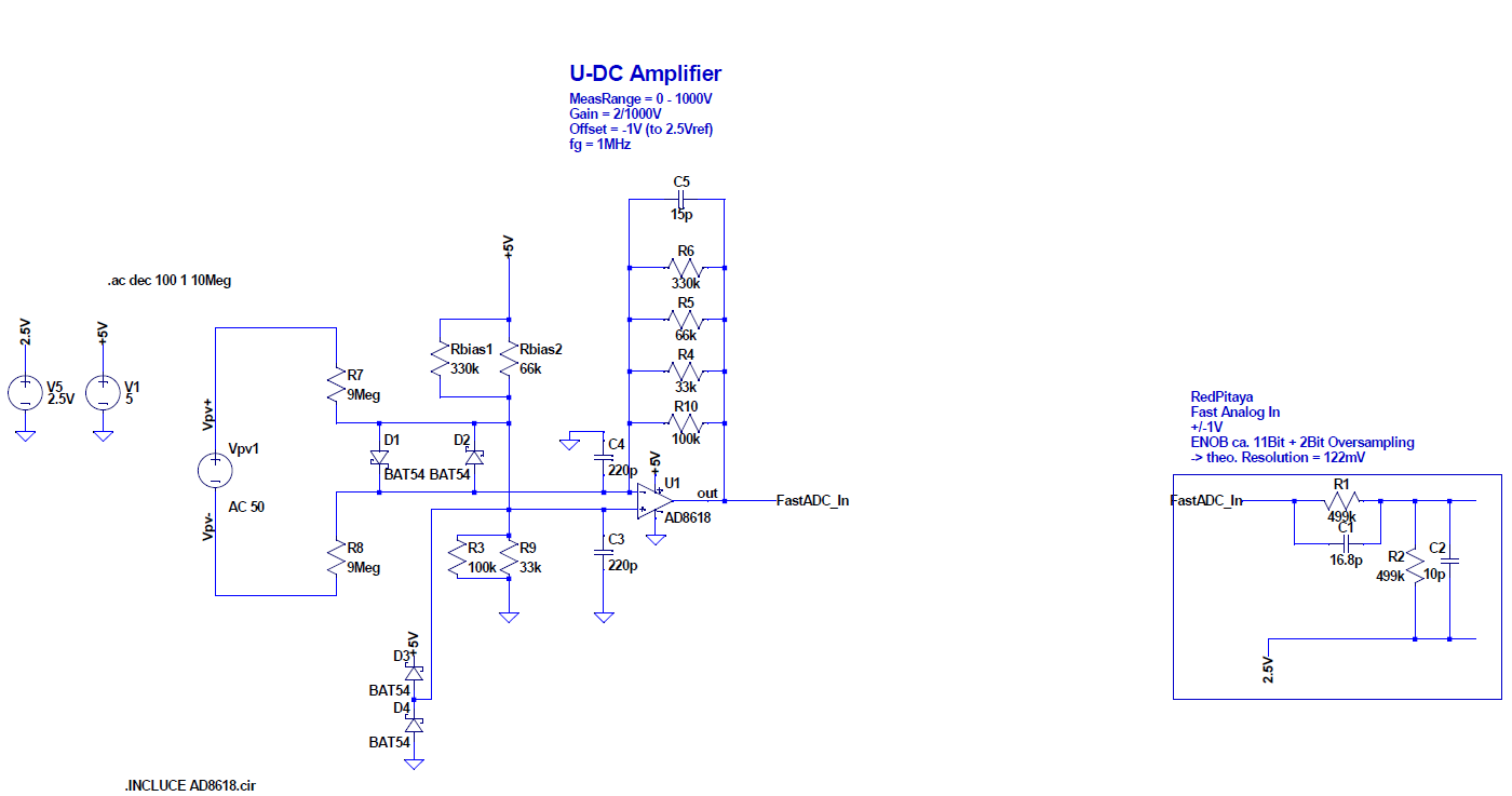
!! Update:
The first pole at around 400 Hz disappears when I connect Vpv- directly to Gnd. Measured frequency response Update
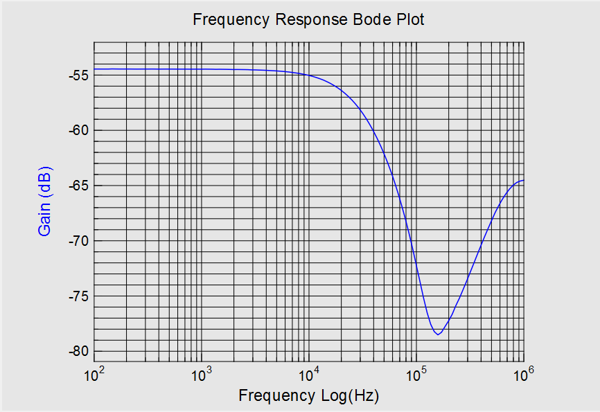
!! Update #2:
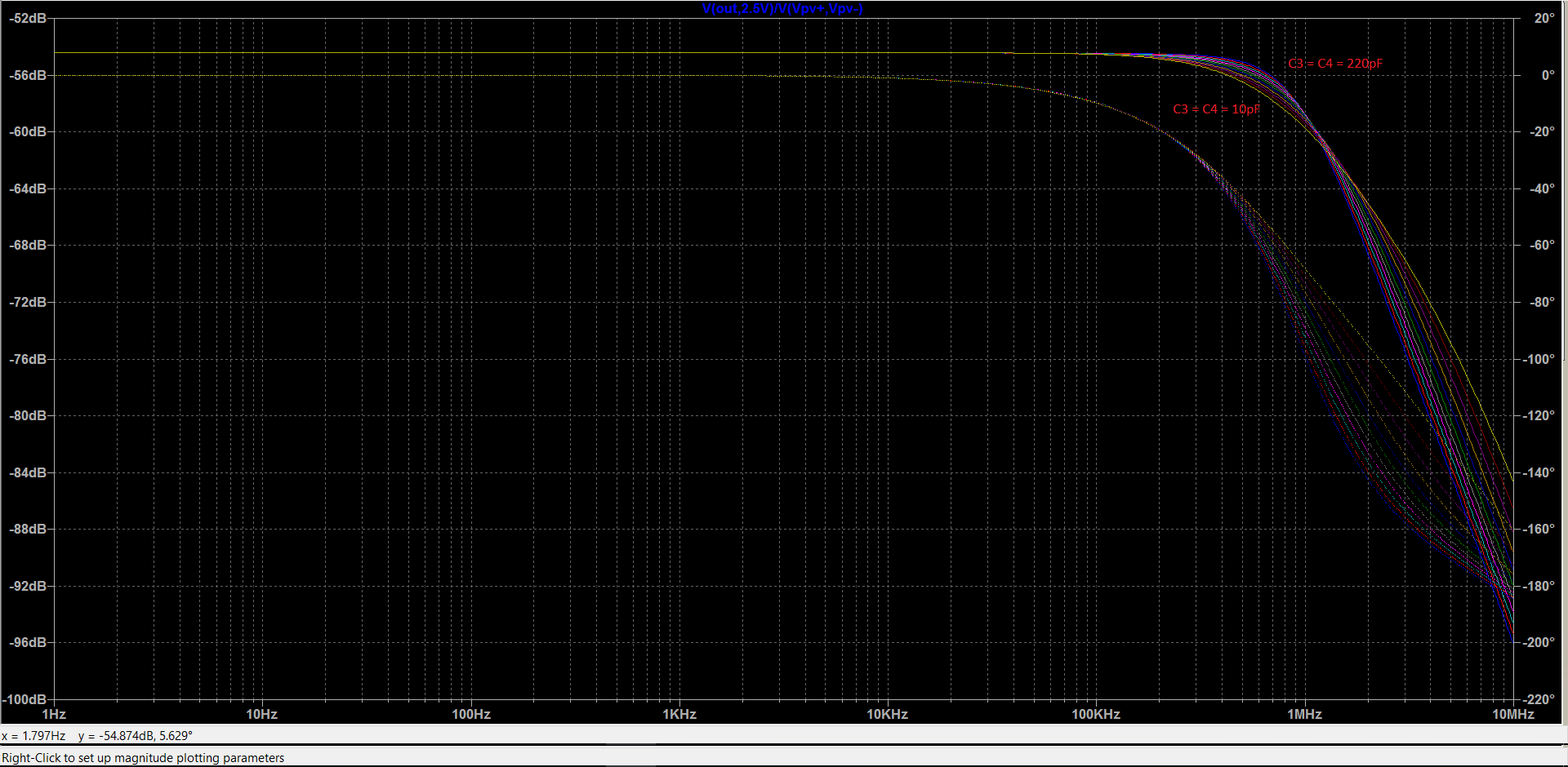
C3 & C4 are there to improve the steepness of the filter. But as andy aka pointed out they drive the gain of the opamp up at high frequencies until the 15pF get active. Could this be the problem?
Could it be possible that the GBP of the opamp wont be enough at high frequencies because the gain also increases? How would I simulate for that? Effect of C3 & C4
\$\endgroup\$
5
  • \$\begingroup\$ In a 10x oscilloscope probe, there is a small capacitor in parallel with the large 9 MΩ resistor to form a capacitive voltage divider in parallel with the resistive voltage divider - is is possible this was omitted in the schematic? \$\endgroup\$
    – W5VO
    Commented Jun 1, 2018 at 14:47
  • \$\begingroup\$ Thank you for your fast response. I tried measureing it with the 1x Setting which adds 13pF // 1MOhm to the output of the opamp and removed the red pitaya but the simulated frequency response stayed the same. \$\endgroup\$
    – JohannesW
    Commented Jun 1, 2018 at 15:04
  • \$\begingroup\$ When simulating the 10x setting 9Meg // 15pF in series to the previously mentioned 1Meg // 13pF the gain increased from 10kHz to 1MHz but there was no notch. \$\endgroup\$
    – JohannesW
    Commented Jun 1, 2018 at 15:07
  • \$\begingroup\$ Did you put proper decoupling capacitors on the supply? \$\endgroup\$
    – lucas92
    Commented Jun 1, 2018 at 15:13
  • \$\begingroup\$ The supply output impedance should be below 50mOhm up to 5MHz. \$\endgroup\$
    – JohannesW
    Commented Jun 1, 2018 at 20:00

2 Answers 2

1
\$\begingroup\$

Surely C4 is in the wrong place: -

enter image description here

It should be across the feedback network and not from -Vin to ground if you want to maintain a balanced amplifier.

I don't see the reason to have C3 and C4 at all. Just putting C4 where it is does not balance the gain to keep it differential - it does nothing except boost the +Vin gain at high frequencies. The AD8618 input capacitance is about 3 pF and 220 pF capacitors are dwarfing that capacitance. You are bound to get problems with them.

\$\endgroup\$
5
  • \$\begingroup\$ link \$\endgroup\$
    – JohannesW
    Commented Jun 1, 2018 at 19:15
  • \$\begingroup\$ If you have something to show why not post it to your question. What I saw was too blurred to read. \$\endgroup\$
    – Andy aka
    Commented Jun 1, 2018 at 19:20
  • \$\begingroup\$ C3 and C4 are in there because of the improved frequency response but yes I think it would probably be smarter to not use them. I am currently storing the sampled data with 8MSps. With C3 & C4 I have a gain of -30dB at 4 MHz while without only -20dB(Not much I know great but I have some CIC decimators that decimate it from 125MSps to 8MSps which also help with the anti aliasing ) \$\endgroup\$
    – JohannesW
    Commented Jun 1, 2018 at 19:20
  • \$\begingroup\$ Sorry pressed Enter on accident while writing the comment. I will put it in the question. \$\endgroup\$
    – JohannesW
    Commented Jun 1, 2018 at 19:22
  • \$\begingroup\$ The bottom line is that with those capacitors you don’t have a mathematically differential amplifier. Short the inputs and drive both inputs together with respect to ground and see how poor it gets at common mode rejection as frequency rises. \$\endgroup\$
    – Andy aka
    Commented Jun 1, 2018 at 19:57
0
\$\begingroup\$

In the actual system (not a simulation), there will be imbalances in capacitance across the two 9MegaOhm resistors. How do you plan to compensate for those mismatches?

\$\endgroup\$
1
  • \$\begingroup\$ Thanks. The 9MegaOhm resistors are actually 9x 1MegaOhm resistors that are already placed very symmetrical for EMI reasons alone. I never expected the 1MegaOhm resistors to have any significant parasitic capacities but according to this group they could have up to 0.1pF per 1Mohm resistor. These values are not critical in my simulation but if they get any higher (x10) the pole they introduce starts to enter the passband. How could I minimise this? \$\endgroup\$
    – JohannesW
    Commented Jun 1, 2018 at 19:57

Your Answer

By clicking “Post Your Answer”, you agree to our terms of service and acknowledge you have read our privacy policy.

Not the answer you're looking for? Browse other questions tagged or ask your own question.