2
\$\begingroup\$

I would be thankful if someone could explain me what is the general formula used to calculate the gain of a common source jfet amplifier.

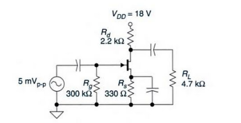
I have the fallowing circuit:enter image description here

Since this circuit was taken out from a book, the author says that:"The voltage gain is equal to gm times the signal resistance in the drain leg. There are two paths to signal ground from the drain terminal.One is through Rd and the other is through RL."

If we make the small signal model we will realise that Rd is in paralel with RL so rd = Rd||RL hence the Gain = gm * rd

Okay, all nice and good but I don't understand that, since we use source degeneration resistor, why we bother ourself calculating the transconductance (gm) in order to calculate the gain, when we could calculate the voltage gain by dividing Rd with Rs ( Gain = -Rd/Rs ) just like in bjt.. Or this formula isn't available anymore at JFET?

Ps: The author of the book assumed a gm of 3mS which after calculating the gain it results a 4.5 voltage gain. If we divide Rd with Rs we will get a voltage gain of 6.6.

Thanks in advance!

\$\endgroup\$
2
  • 2
    \$\begingroup\$ The source resistor is bypassed by the capacitor which in a simple analysis would be assumed to have zero impedance at the frequency of interest. If the source resistor was not bypassed the gm would be reduced as you say. \$\endgroup\$ Commented Jun 13, 2018 at 15:43
  • \$\begingroup\$ The mentioned formula gain=-Rd/Rs is a rough approximation only and can be used for Rs>>1/gm only. This restriction applies also to the BJT case. In your circuit the resistor Rs is bypassed by a capacitor and does not appear in the gain formula (if Cs is sufficiently large). \$\endgroup\$
    – LvW
    Commented Jun 13, 2018 at 15:48

2 Answers 2

5
\$\begingroup\$

The mentioned formula

gain=-rd/Rs

is a rough approximation only and can be used for Rs>>1/gm only (without any bypass capacitor). This restriction applies also to the BJT case. In your circuit the resistor Rs is bypassed by a capacitor and does not appear in the gain formula (if Cs is sufficiently large).

Here is the correct formula:

gain=-gm * rd/(1+gm * rs)

with rs=Rs||(1/jwCs).

As you can see, for rs<<1/gm the formula reduces to gain=-gm * rd.

In contrary, for Cs=0 and Rs>>1/gm the mentioned gain formula reduces to gain=-rd/Rs (as mentioned at the beginning).

\$\endgroup\$
3
\$\begingroup\$

FOR THE IMPATIENT: Skip to Point 6, the formula.

  1. Just as with BJTs, we must account for the internal resistance of the JFET source. For the JFET, this resistance is 1/Gm (Gm in Siemens or mhos). (For BJTs, use Shockley’s Constant, 26/Ic, in mA. The answer to this equation is in series with the external emitter resistor.)

  2. Point #1 suggests a revised formula for JFETs: Vg= (Rd || Rl) / (Rs + Rs_internal). Yet life isn’t this simple.

  3. We must also account for the source capacitor Cs. Two problems here: (A) The source cap does not bypass the internal source resistor Rs_internal. (B) Despite the argument that Cs “eliminates Rs,” Cs does not do that. In fact, Cs: (C) Eliminates the JFET’s DC amplification capability. (D) Renders the JFET nonlinear, by introducing a high-pass response curve.

  4. To account for the high-pass curve, we must select the frequency where we want to measure Vg. (Typically 1 KHz.) For example, the Vg at 100 Hz will be much smaller than the Vg at 1 kHz. The Vg at DC will be about zero. (DC-Vg depends on the leakage resistance of Rs.)

  5. We can reduce, but not eliminate the high-pass effect by increasing the Cs value. The ideal value will be expensive. But it won’t eliminate the problem.

  6. Proposed new Vg formula: [(Rd || Rl) / ((Csx || Rs) + 1/Gm)], where Csx is the capacitive reactance of Cs, in ohms, at the frequency of Vg measurement. Or: Use 10% of The R2 value, in ohms.

  7. There are other factors that affect Vg. For example, I’m ignoring (A) Internal capacitances. (B) RCL of circuit wiring. (C) Typical variability over a 5X range of name-brand JFET parameters. (D) Gm measurement at a different Id/Vg curve than what the subject circuit is using. (E) The unknown-unknowns.

  8. If we don’t know the value of 1/Gm: Use the value of Rs, in ohms. (See Albert Malvino, Transistor Circuit Approximations, 3rd ed.)

\$\endgroup\$

Your Answer

By clicking “Post Your Answer”, you agree to our terms of service and acknowledge you have read our privacy policy.

Not the answer you're looking for? Browse other questions tagged or ask your own question.