1
\$\begingroup\$

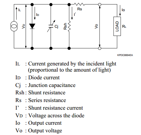
What can I learn from an equivalent circuit model of photodiode like the following?

Diode

I've actually gone the whole way beginning from doping semiconductors through each noise term to the amplification gain.

Now I'm at the application stage and I stumbled over this circuit and noticed it is quite common. But since I don't see any technical purpose of it, I guess it is constructed to understand the photodiode itself in a technical way. But what does it tell me really? And why is nearly everything parallel to each other?

I've seen this EE.SE question (equivalent circuit for solar cell) which is quite connected, but doesn't touch it directly. However, it hasn't been answered yet anyways.

edit

To be more precise: I'm more interested in the circuit itself and less in the single parts of it. I probably can google each part of it but what is about the circuit itself?

\$\endgroup\$
1
  • \$\begingroup\$ The circuit appears to speak for itself. If your question was "what is the effect of junction capacitance" then your question can be answered. \$\endgroup\$
    – Andy aka
    Commented Jun 14, 2018 at 12:00

2 Answers 2

3
\$\begingroup\$

What can I learn from an equivalent circuit model of photodiode

I believe you are overthinking this a little bit. While a model may not be of any use in let's say a technical datasheet, it can be pretty useful for designing circuits or perhaps research purposes. It also serves as a kind of mental image of a photodiode. People are usually graphically oriented, and models usually help to make sense of stuff.

Another important use for models, is to investigate how a photodiode would work in conjunction with other circuitry (eg. a transimpedance amplifier - TIA). We can use a model like this construct criteria and trade-offs that may prove necessary for the application. For example, the junction capacitance turns out to be very important for the stability of a TIA. From the model you can also see that \$R_s\$ could decrease the bias voltage, possibly increasing rise and fall times of the photocurrent. The photocurrent seems to be best modeled by an ideal current source, telling us that the bias voltage probably doesn't have much influence on the (DC) photocurrent. Etc.

Another use for a model is inside simulations. A Spice simulator usually doesn't include a model for photodiodes, and as such we may need to model it ourselves similarly to the schematic in your question.

And why is nearly everything parallel to each other?

It just turns out that that is the best way to model a photodiode. There is actually little choice involved. We just identified certain parasitic effects, and when modeling them it seems to be best represented by shunted components.

\$\endgroup\$
2
  • \$\begingroup\$ Thank you! I just noticed that not each part of the circuit is part of the diode itself.. but I'm wondering about your statement that the bias voltage probably doesn't have much influence on the (DC?) photocurrent. From my understanding it's all about the bias voltage (in case of reverse bias). \$\endgroup\$
    – Ben
    Commented Jun 15, 2018 at 6:54
  • \$\begingroup\$ If all photocarriers are generated inside the depletion region then it doesn't matter what the bias voltage is, the responsivity will remain constant and the speed will change. But yes, in general the responsivity will be affected by the bias. But I felt that this was outside the scope of your question so I kept it to this crude approximation. \$\endgroup\$
    – Sven B
    Commented Jun 15, 2018 at 8:03
1
\$\begingroup\$

And why is nearly everything parallel to each other?

It is how someone modeled a semiconductor junction which incident light generates a current, where the junction capacitance is vital and where some leakage currents are observed empirically. Sometimes models gobble up some of the insight.

Also, it seems that the resistors are there for this particular configuration. In most cases that I have observed, a photo diode is reverse biased (for greater photon conversion efficiency), which would render R_sh unsatisfactory, since it would lead to a DC current through the junction.

\$\endgroup\$
2
  • \$\begingroup\$ Thank you, can you please explain the unnecessary R_sh a bit more? Why does a reverse biased diode cause a DC current through the junction? I mean, depending on the bias voltage, in reverse as well as in forward direction a current will flow there. \$\endgroup\$
    – Ben
    Commented Jun 15, 2018 at 6:57
  • \$\begingroup\$ Well when the diode is reverse biased, that R_sh might be removed it if is large in value. The model might not be still usable in the reverse bias condition and DC bias. It might also be a model that DC voltage components are all eliminated, and only the effect of DC bias to Cj and IL is applied and used accordingly. They are all about what is deemed the most important in the phenomenon that is to be caught in the model. \$\endgroup\$ Commented Jun 15, 2018 at 8:09

Your Answer

By clicking “Post Your Answer”, you agree to our terms of service and acknowledge you have read our privacy policy.

Not the answer you're looking for? Browse other questions tagged or ask your own question.