4
\$\begingroup\$

I’m designing a low power wakeup receiver (WuRx) circuit that will be used to wake up an Arduino and its 433 MHz transceiver, both of which pull way too much current (tens of milliamps) to keep running at each remote node. The goal is to develop a low power wake up receiver / detector that will wake up Arduino (or any sleeping MCU) when RF wake up signal is present. The RF wake up signal will be a series of brief OOK pulses from the transmitter.

I need to amplify the UHF signal from its ten microvolt antenna level, to at least 100 millivolt to 1 volt level in order to detect the RF envelope via a simple diode rectifier, which will then trip a comparator indicating “RF present” during OOK (on-off keying). These pulses will then be counted using some flip/flops or a counter within a given time window to detect a valid wake up signal.

I have done extensive research on these wake up receivers and prior art. Traditional conversion of RF to IF results in too much quiescent current due to the LO current. This has led me to conclude that a low power RF amp fed by a ceramic bandpass filter can solve this problem.

Since this is simply an RF wake up detector, linearity during amplification is much less important than very low quiescent current when no RF is present. These IoT style slave sensors typically sit idle 99.999% of the time, only needing to awaken for a few tens of milliseconds whenever the master polls them.

The flow will look something like this:

Antenna -> Bandpass Filter -> RF Amp -> OOK Envelope Detector -> Wakeup Interrupt to Arduino -> Transceiver Wakeup -> Rx Data -> Process Rx Data -> Back to Sleep

My problem is how to minimize the quiescent amplifier current drain (to nanoamp level ideally) yet sufficiently amplify the microvolt signal once its present and coming out of the bandpass filter. Total amplifier current drain when RF signal is present can be a few milliamps. I’m thinking several 15 dB to 20 dB amplification stages in series to yield a 10,000 to 100,000 x signal boost should be sufficient; e.g. 10 uV to 100mV - 1V.

I’m looking at LNA transistors like the BFP720, a low noise silicon germanium BJT, but willing to consider all low cost options. Low cost and small footprint are also factors but low quiescent current consumption on 3V battery power is critical.

I’ve tried Class C amplifiers with resonant circuits but simulations are failing (using SystemVision simulator) due to low (millivolt) level input signals being too tiny to allow the transistor to conduct. What type of amplifier can I use that has very low quiesce bias current and can amplify this tiny UHF signal?

If I can figure this out, it will help a lot of folks out who are struggling to solve this type of low power wake up problem.

Thanks in advance for guidance.

\$\endgroup\$
6
  • 1
    \$\begingroup\$ I don't think you'll find one. But for (relatively) low power simple receivers you might take a look at super-regenerative circuits. \$\endgroup\$
    – user16324
    Commented Jul 8, 2018 at 20:12
  • \$\begingroup\$ Even if you get this working, I'd be worried about spurious activations waking up the processor often and costing power. Worse, many available super-regens for data applications toggle from one rail to the other in the absence of real signal, and assume software on a mains-powered MCU is looking for meaning. \$\endgroup\$ Commented Jul 8, 2018 at 20:26
  • \$\begingroup\$ So don’t mind the wake up from any signal sharing this BW? \$\endgroup\$
    – D.A.S.
    Commented Jul 8, 2018 at 20:58
  • 1
    \$\begingroup\$ I plan to require a series of on-off keying pulses to wake up the MCU. Other signals, noise, etc. should be ignored if not matching the required wakeup pattern. Once I can decode the OOK signal, I can use a unique wakeup pattern created by the OOK transmitter. \$\endgroup\$
    – rbraddy
    Commented Jul 8, 2018 at 22:19
  • \$\begingroup\$ @rbraddy and what is going to decode the sequence? Traditionally that is the job of the MCU, so hopefully you have very fine grained sleep/wake resolution. Unfortunately regens often toggle fairly frequently in the absence of signal - you'd almost need something like a hardware timer that generates a wake interrupt only when it doesn't get a transition before overflowing. \$\endgroup\$ Commented Jul 8, 2018 at 23:20

4 Answers 4

1
\$\begingroup\$

This is another "not an answer" :) I do not have enough experience to suggest a circuit.

There are hundreds of very low power (down to 300 nA) single-supply Op Amps. Have you considered these instead of transistors?

Furthermore, the same Op Amp can become part of active bandpass filter, reducing number of components and possible power draw too.

UPDATE

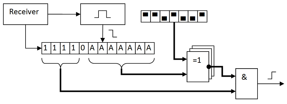
Re address decoding, here is an idea of a protocol that should be easy to implement with simple logic components:

  • The transmitter encodes target address as follows:
    1. Node IDs are selected from a subset of natural numbers with less consecutive "1"s than chosen "trigger" length. Let's say trigger is 4 bit long.
    2. "0" is transmitted, followed by node ID, using pulses of two different lengths. Let's say long pulse for "1" and short for "0".
    3. "0" is transmitted, followed by the "trigger" as group of "1"s, e.g. "01111"
    4. Note that transmission frequency is constant, so shorter pulses are followed by longer pauses and v.v.
  • The receiver is connected to monostable multivibrator triggered by rising edge of a signal. Multivibrator generates pulse that is longer than "0" and shorter than "1".
  • The falling edge of the multivibrator is used as clock for shift register, while the receiver output is used as data input.
    1. The end result is that shift register contains node ID, 0 and the trigger.
    2. At no time the register has 4 consecutive "1"s until entire packet is received.
  • The trigger bits of a register are connected to AND gate. The address bits are compared to address selection DIP switch with XNOR (or XOR, does not matter) gates and the outputs are fed to the same AND gate. The output of the gate is wake-up signal.

This approach has the benefit of fixed packet length and no need for synchronous clock. 8-bit address can be implemented with as few as 3-4 ICs. Below is simplified diagram.

enter image description here

The output can be used as wake-up or to control power switch. With power switch MCU will be running until you send a different address. With wake up you can add "waiting time" to MCU logic then wake up several of them and transmit to all of them simultaneously.

Oh, and all the signals can be inverted, of course. For example the presence of RF carrier can be used to power-up decoding logic and then Off pulses will transmit the address.

UPDATE 2

I was in the process of typing some additional thoughts when I saw that link in the comments. Very interesting read indeed, by itself and some references too. It has helped those thoughts to crystallize into these key design points:

  • For this application the design of the RF stage is just as important as selection of the low-power components. All the known tricks to maximize antenna gain should be used. For example, directional antenna increases reception from the master node while at the same time significantly reduces interference, thus minimizing false wake-ups.

  • Staged power management. This means breaking signal processing into multiple steps by power requirements so that the power to next stage is only applied when the signal conforms the criteria of the previous stage. I am not particularly impressed by the use of comparator and SPI interface in the article. They both require power too early in the processing chain. Just as they use preamble to generate wake-up for the processor, the presence of RF carrier for a certain period can be used as criteria for powering up the comparator. The output from comparator and preamble detector can be used to power up address decoding logic, and so on.

  • Integrated RF signal. Voltage doubler is good, but why stop there? It could be possible to use multiple diodes or MOSFETs to build charge pump with enough power to satisfy your distance requirements. The basic idea here is that sacrificing data rate by increasing pulse duration allows RF stage to build-up voltage to useful levels. This also means inverted OOK modulation (i.e. using pauses as data pulses) is preferable. Also, as low as power consumption of MCU can be, the address detection with logic chips might still be more efficient, and can be done faster (MCUs typically require hundreds of cycles to wake up from deep sleep).

\$\endgroup\$
14
  • \$\begingroup\$ Great point. I didn't look carefully at Op Amps as I assumed they wouldn't handle the UHF frequencies, but it makes sense to look at them more carefully. \$\endgroup\$
    – rbraddy
    Commented Jul 9, 2018 at 19:26
  • \$\begingroup\$ Ah, I see. Well, there are Op Amps with GBWP up to 18 GHz, but you'll be looking at something like 0.9 mA then. On the other hand you can intentionally choose Op Amp with lower GBWP to establish low-pass side of bandpass filter. \$\endgroup\$
    – Maple
    Commented Jul 9, 2018 at 20:48
  • \$\begingroup\$ I'm seeing the same thing. The UHF GBWP Op Amps current drain is well beyond what I need, which is a few microamps of idle current with no RF present. \$\endgroup\$
    – rbraddy
    Commented Jul 9, 2018 at 22:06
  • 1
    \$\begingroup\$ We are getting into the ballpark here. This discussion on Op Amps and address decoding has led me to a 2011 paper where this problem was solved without an RF amplifier stage using Schottky diodes in s voltage doubler detector configuration. elucidare.co.uk/assignments/project_WUR/05992833.pdf \$\endgroup\$
    – rbraddy
    Commented Jul 10, 2018 at 3:22
  • 1
    \$\begingroup\$ LOL Microsoft Office Word 2007 :D \$\endgroup\$
    – Maple
    Commented Jul 10, 2018 at 16:11
1
\$\begingroup\$

I solved this problem for a commercial product I worked on using a CC1101 transceiver, although other similar devices would also work. The device was battery powered and needed a 5+ year life from a single cell.

The receiving device would power its transceiver up in RX mode every 2 seconds, wait a while and then power it down. The CC1101 has a built-in function to do this, but the Arduino could do it manually too.

The awake time for the transceiver is kept as low as possible, IIRC it was about 20ms. Just long enough for the oscillator to stabilize and a wake-up signal to be received.

The transmitter would send a 2.5 second wake-up signal consisting of 0x55 bytes. Reason for choosing 0x55 is that it's alternating 1s and 0s in binary, and with RF you need to balance the numbers of ones and zeros for most transmission schemes. This was using the CC1101's default FSK mode, if I recall.

The 2.5 second burst is guaranteed to overlap the 2 second periodic check for wake-up signals. Once woken the receiver waits for commands and then goes back to sleep.

I can't remember the exact numbers for power consumption, but with that scheme running 24 hours a day the battery life was well over 5 years from a 4000mAh cell, and that included all the other work that the device had to do periodically. I think the radio side accounted for about a third of the total energy budget.

\$\endgroup\$
0
\$\begingroup\$

This is not an answer to your wake-up receiver problem, but have you thought about doing it the other way round?

You were talking about a master node, so I assume you have a star topology with one master node without power requirements and several slave nodes with strict power requirements?

What about instead of polling the slaves with the master you just periodically wake up the slaves with a low power timer running on the MCU and transmit the data to the master, which is always listening?

Advantages:

  • No need for a wake-up receiver
  • sleep power consumption in the microwatts range
  • no spurious wake-ups

Disadvantages:

  • Can't poll the slave nodes outside their regular transmit schedule
\$\endgroup\$
4
  • \$\begingroup\$ Yes, the issue with this is latency of opportunity to push an unsolicited message into a receive window following a node-timed transmit. You may be able to get down to a second or less however. With good clock synchronization you may be able to make the node transmissions less frequent than the receive windows, or only do them (or some kind of temporal search of receive windows) if an expected heartbeat is not received in an occasional window. However, when the system has lost sync, latency could be extreme since first the sync loss must be detected, and then re-sync must happen. \$\endgroup\$ Commented Jul 8, 2018 at 23:20
  • \$\begingroup\$ Polling takes far too much power. Each node will only be commanded to change a few times per hour, then perhaps not at all for a week or two. Polling will soak the battery at each node massively. The master broadcasts to all nodes simultaneously, further reducing power. \$\endgroup\$
    – rbraddy
    Commented Jul 9, 2018 at 0:53
  • \$\begingroup\$ You are right, but I guess it all depends on your latency requirements. If your circuit is drawing f.e. 20mA for 20ms every 20 seconds that equals an average power consumption for polling of only 20uA. \$\endgroup\$ Commented Jul 9, 2018 at 1:09
  • \$\begingroup\$ Yeah, latency needs to be no more than a couple of seconds when user is engaged with the system. \$\endgroup\$
    – rbraddy
    Commented Jul 9, 2018 at 1:30
0
\$\begingroup\$

After further digging, I have discovered what appears to be the answer to the original question - what kind of amplifier has low quiesce bias current that can amplify a tiny UHF signal. The answer turns out to be non-obvious and arose from RFID tag research:

Quantum Tunneling Reflection Amplifiers.

According to this Georgia Tech dissertation, tunneling reflection amplifiers using low quiescent bias in the 20 uW range are capable of amplifying microwave signals from the -85 dBm level with modulation bandwidth up to 7 MHz, extending RFID tag range up to 1.2 km.

https://smartech.gatech.edu/bitstream/handle/1853/58228/AMATO-DISSERTATION-2017.pdf#page49

The biggest challenge appears to be how to create the accurate mV level biasing required from a 3V battery supply and maintain it over the full required temperature range. Bias is 60 mV at 340 uA, so some efficienct means of reducing 3V to 60 mV - buck dc-dc converter?

In any event, this looks promising. If it worked that well at 5.8 GHz for RFID should be fine at 433 MHz.

\$\endgroup\$
6
  • \$\begingroup\$ Have you looked at MMIC devices, like BGA6130? 4 uA sounds promising \$\endgroup\$
    – Maple
    Commented Jul 13, 2018 at 6:23
  • \$\begingroup\$ Yes. On the surface looks promising but the 4uA is shutdown mode, normal operation uses 40 to 70 mA. MMICs power consumption down into 4 mA range are available but nothing yet with low quiesce current with no input signal and sensitivity below -50 dBm. All I have found want -21 dBm or more input signal level. Thanks for continuing the hunt with me. \$\endgroup\$
    – rbraddy
    Commented Jul 13, 2018 at 13:43
  • \$\begingroup\$ What might work would be to have a “predetector” that can determine there’s a faint signal present in the passband (it made it through the bandpass filter on the front-end), down in the mud at -80 dBM or so, then use that predetection to enable a low-power amplifier like the MAX2634. This way, we only amplify when there’s someone knocking. This would increase the costs of detection and wake up but increases the sensitivity. That’s a way to leverage @maple suggestion. \$\endgroup\$
    – rbraddy
    Commented Jul 13, 2018 at 20:43
  • \$\begingroup\$ I have enough to begin prototyping to research and validate various ideas and potential options. Thank you for all the help. \$\endgroup\$
    – rbraddy
    Commented Jul 13, 2018 at 21:49
  • \$\begingroup\$ Good luck! And post the results when you are done, please. Very curious how it turns out. \$\endgroup\$
    – Maple
    Commented Jul 13, 2018 at 21:51

Your Answer

By clicking “Post Your Answer”, you agree to our terms of service and acknowledge you have read our privacy policy.

Not the answer you're looking for? Browse other questions tagged or ask your own question.