3
\$\begingroup\$

Primarily for academic interest (so please don't suggest ICs to do this, as they won't help me learn how to deal with this kind of problem) I'm attempting to design a buffer circuit to accept a digital differential signal with input voltage swings between 0.6V and 1.5V frequency up to 250MHz and reproduce the signal with the output voltage swing normalized to 1V. I'm working with a 3.3V supply, and am aiming to have the signal centred at approximately 2V (although this isn't a hard constraint, so don't mind if this varies by a fair amount). I'd also like to keep power consumption to a minimum.

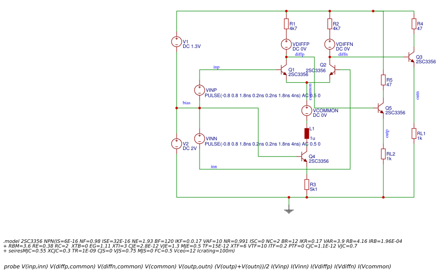
What I've got so far is this schematic:

schematic

The voltage supply is split so I get 3.3V, 2V and 0V rails (the 2V rail is used as a reference for my inputs and for biasing a current source circuit). Q1 and Q2 are a differential amplifier, accepting the input signals 'inp' and 'inn'. Their common emitter is referenced to a current source calibrated to sink roughly 0.3mA. I originally didn't include L1 in this arrangement, but transients during transitions were rather high, and I was seeing quite a bit of overshoot beyond my target rails, and a small inductance seemed to solve these problems.

The outputs of the differential amplifier are then buffered through a pair of transistors that are allowed to draw higher current, and into a load (simulated by a pair of 1K resistors to ground in this schematic).

The 0V voltage sources are used for current measurement; apparently this is the standard way of doing this in ngspice, which I'm using for simulation.

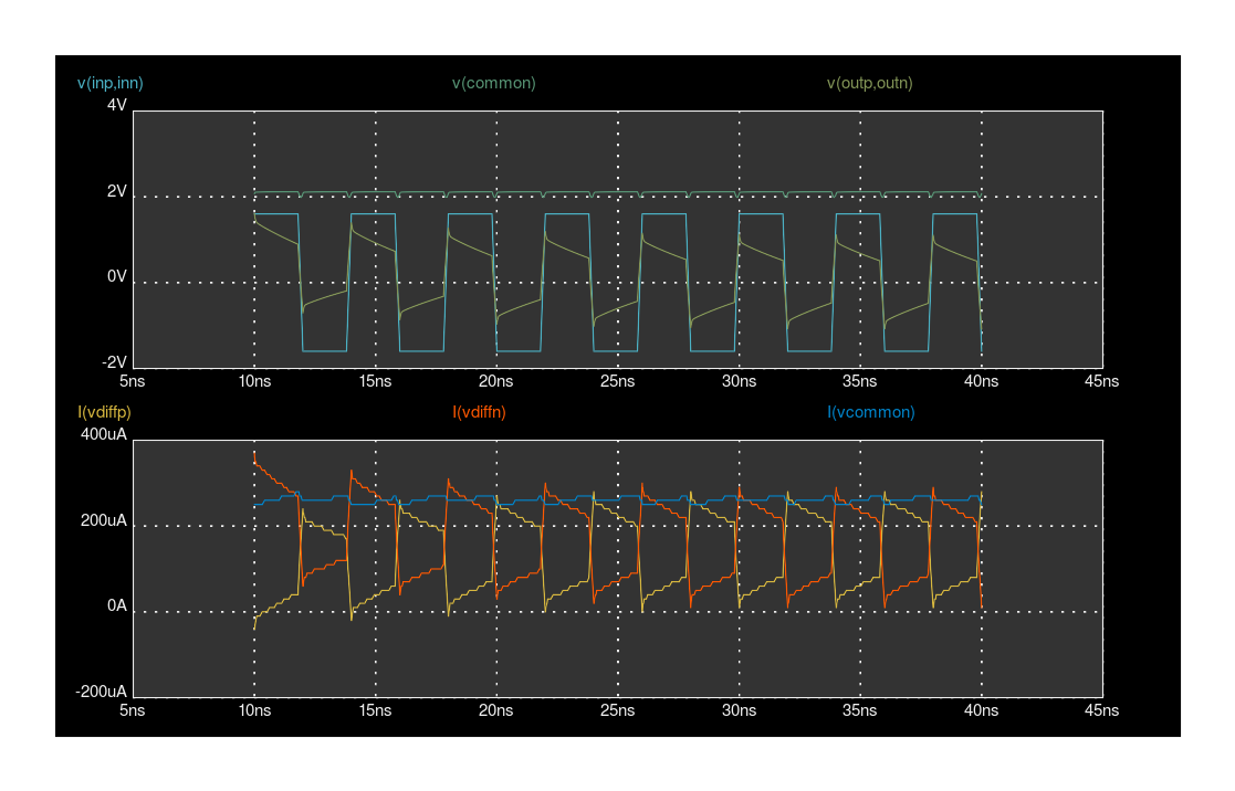
The results of this aren't quite what I was expecting. The results of a transient simulation are shown below:

transient simulation

With each transition, my output signal hits approximately the 1V swing I was aiming for, but then it rapidly fades back towards the mean output level. It looks as though some stray capacitance is causing the issue, but I have no idea where it could be coming from. The transistors I'm using (2SC3356) are designed for high frequency applications (fT = 7GHz) so should be perfectly capable of operating correctly in this application. I'm at a loss as to what else could be wrong.

\$\endgroup\$
4
  • \$\begingroup\$ What did you expect with 1uH? I think your assumptions are false. First learn how commercial Diff Amps work such as CML then you will have the best results in design. This is faster than trial and error \$\endgroup\$
    – D.A.S.
    Commented Jul 13, 2018 at 17:40
  • \$\begingroup\$ My assumption was that the important thing was to ensure that the current flow out of the differential pair was approximately constant, which it wasn't to start with but was achieved by adding the inductance. I still don't see why this approach is wrong, though. \$\endgroup\$
    – Jules
    Commented Jul 13, 2018 at 18:04
  • \$\begingroup\$ (I know that this isn't the usual approach taken in the design of ICs, but my understanding is that inductors are tricky to create in ICs, and assumed that this is why such designs tend to prefer more advanced current sources with multiple transistors instead) \$\endgroup\$
    – Jules
    Commented Jul 13, 2018 at 18:27
  • 1
    \$\begingroup\$ @Jules Look at the slope of your output signal. You should see approximately a \$500\:\text{mV}\$ droop over a period of about \$2\:\text{ns}\$. Your current source at the bottom is producing about \$\frac{2\:\text{V}-700\:\text{mV}}{5.1\:\text{k}\Omega}\approx 250\:\mu\text{A}\$. These facts imply a capacitance of \$\frac{250\:\mu\text{A}}{250\:\frac{\text{V}}{\mu\text{s}}}\approx 1\:\text{pF}\$. Note that this happens to be in the vicinity of \$C_\text{re}\$ for your BJT. \$\endgroup\$
    – jonk
    Commented Jul 13, 2018 at 22:12

1 Answer 1

1
\$\begingroup\$

Thanks to the comments above, I realised my main problem was that I was trying to run with the current too low, and this was causing a long delay in the output, leading me to not notice that I had unintentionally inverted the outputs.

Increasing the bias current to 1mA made everything work a lot better (and made it clear that the hack with the inductor wasn't really necessary, as once the circuit was working better it didn't have any useful effects).

Indeed, it turns out the for a circuit of this nature having a stable current sink isn't actually all that helpful. Which just shows that reading about analogue amplifier design when you're designing a digital circuit isn't necessarily all that useful.

\$\endgroup\$
1
  • \$\begingroup\$ I had added a short thought to my comment, about increasing the current, but decided to allow you to figure that out on your own. So I removed it a minute later. +1 for working it through! \$\endgroup\$
    – jonk
    Commented Jul 14, 2018 at 18:09

Your Answer

By clicking “Post Your Answer”, you agree to our terms of service and acknowledge you have read our privacy policy.

Not the answer you're looking for? Browse other questions tagged or ask your own question.