In Sedra and Smith: Microelectronics Circuits (6E), it is mentioned, on page 185:
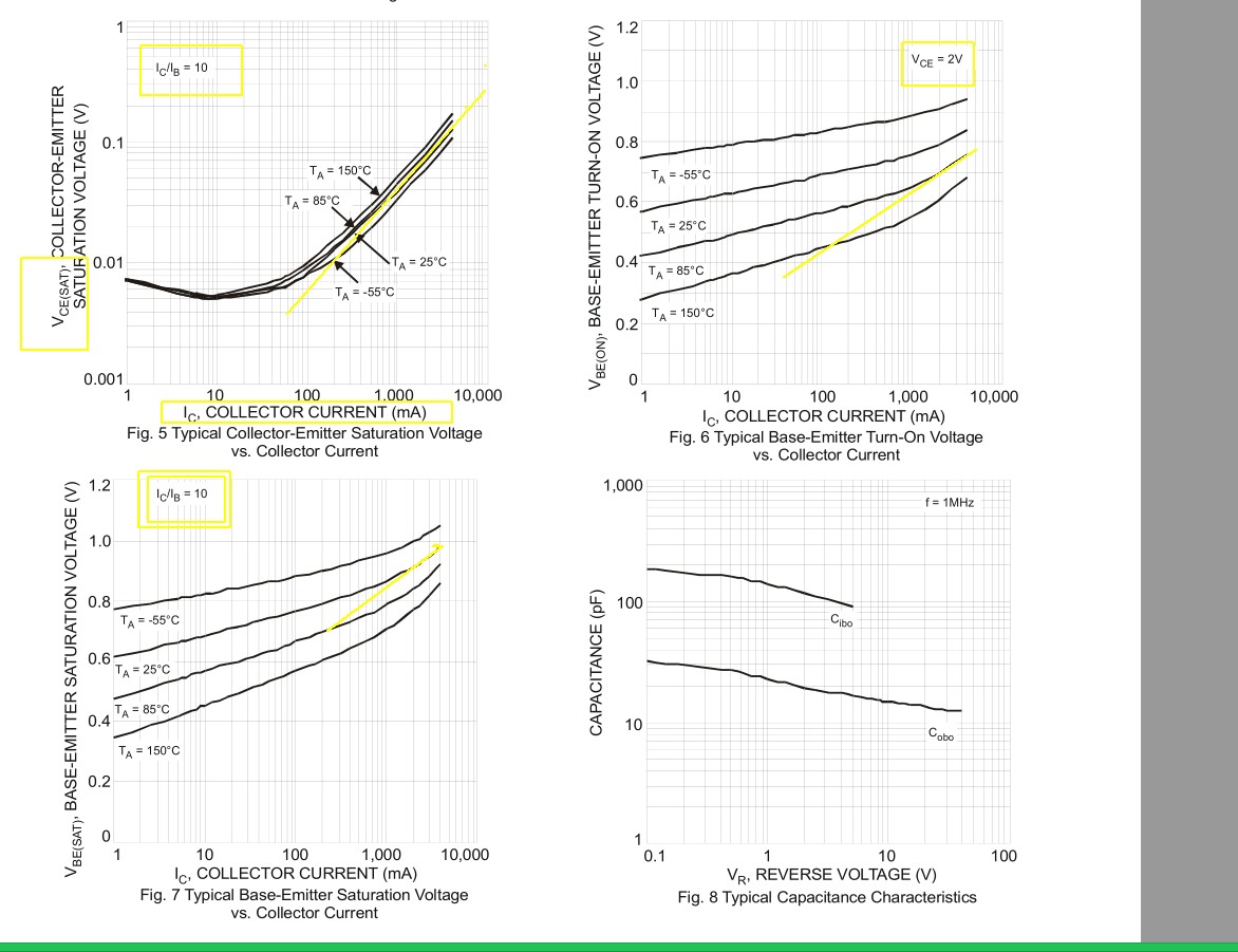
Recalling that the CBJ is much larger than the EBJ, the forward-voltage drop \$v_{BC}\$ will be smaller than \$v_{BE}\$ resulting in a collector-emitter voltage, \$v_{CE}\$, of 0.1 V to 0.3 V.
Why does a difference in junction area causes a change in the forward-voltage drop? A similar question was asked on the site, however, it did not help.
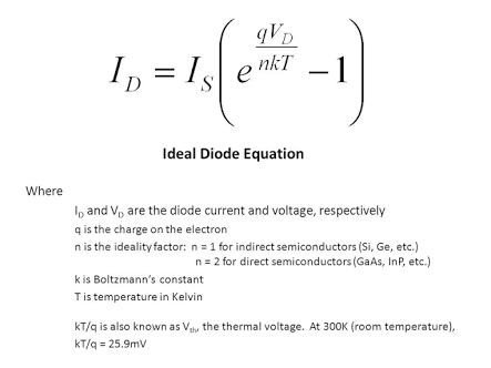
So, I tried using Ebers-Moll model and that is where I am actually getting stuck. So, my question is this:
How should I apply Ebers-Moll method for a transistor working in a saturation region, to get the equation for \$V_{ce}\$?
So far, I know that there are three major Ebers-Moll models, here. I also read that the \$I_{s}\$ is a property of the emitter-base junction.
Additionally, \$i_{c} \leq \beta i_{b}\$.
Thank you for your time. Please inform me if some additional information is needed.


