1
\$\begingroup\$

I'm trying to convert 1.5V logic levels from a caliper data port to 3.3v to be able to read it with a microcontroller, using one of the sparkfun logic level converters. The product page mentions it can be used for 1.8V logic levels, so I was hoping 1.5V would work as well.

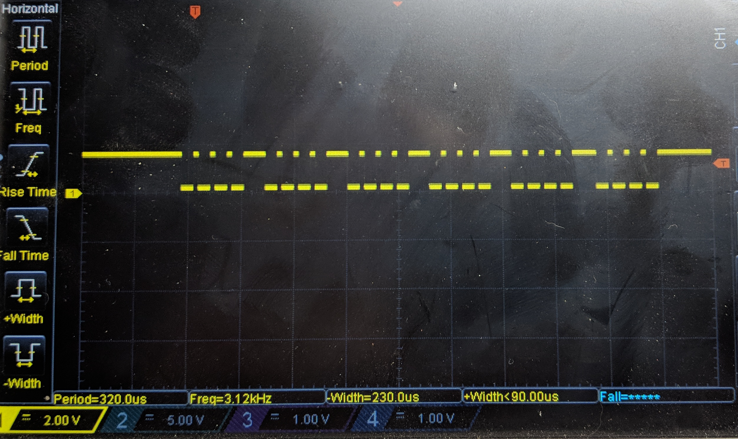
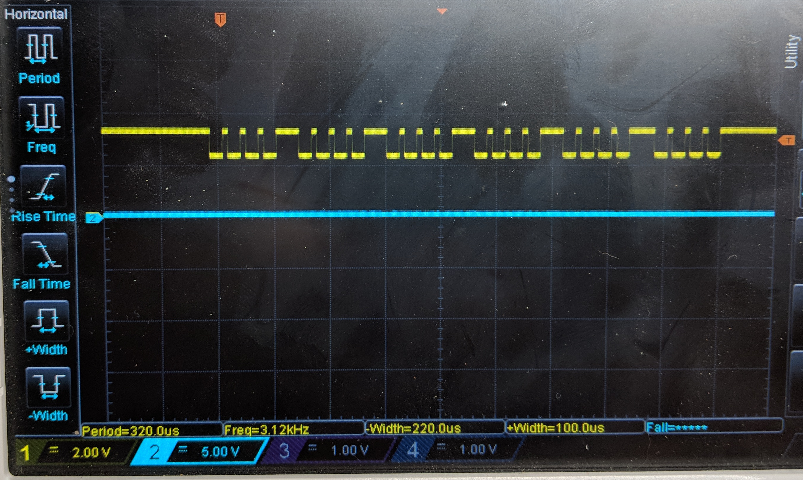
When I look at the waveform generated on the HV side, the high logic level is at the expected voltage, but the low logic level is much higher than expected, and I'm not sure why.

Interestingly, if I connect the LV side directly to the ground and 1.5V from the caliper's data port, the HV side shows 0V and 3.3V as expected

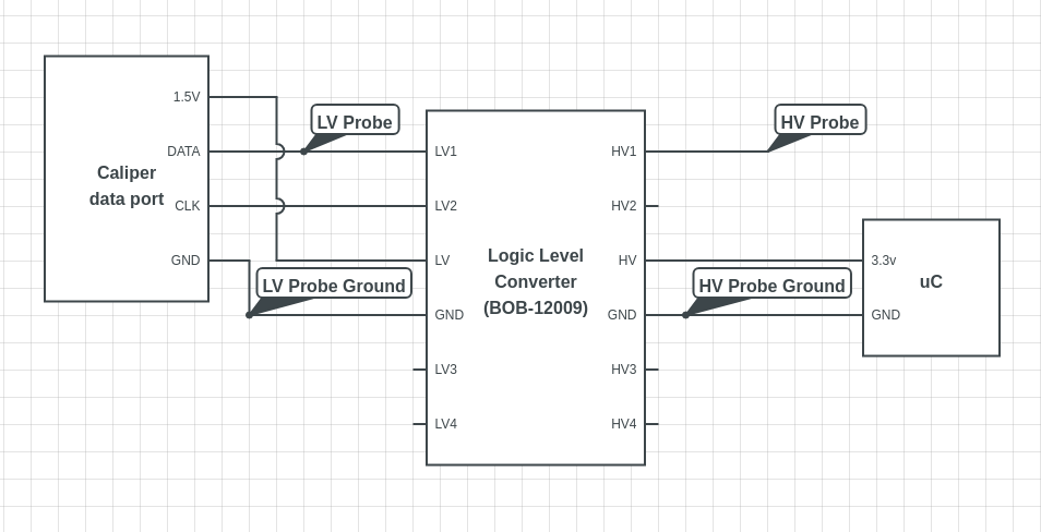
I have it hooked up like so. Note: the probe was actually connected to the CLK pin on both sides (LV2/HV2), not the data pin as shown. Although I got similar results when looking at the data signal.

enter image description here

And here are the traces from the LV side and the HV side.

(LV) enter image description here (HV) enter image description here

I eventually got it working by using a rail-to-rail opamp instead, since I only need unidirectional conversion, but I'd like to understand why I was seeing unexpected results with this. And why connecting the LV side directly to ground produced different results than the low logic level from the clock/data pins.

My best guess is that maybe the clock/data pins from the caliper are unable to sink much current when in a low logic level state?

\$\endgroup\$
9
  • \$\begingroup\$ It is not clear where power for low voltage side coming from. The 1.5V on a "caliper" looks like power input, not output. Any datasheet? \$\endgroup\$
    – Maple
    Commented Aug 18, 2018 at 21:34
  • \$\begingroup\$ The caliper is normally powered from a little button cell. As far as I can tell, the ground and voltage pin on the data port are directly connected to the battery. So you can also remove the battery and power the caliper with an external 1.5V source via the data port. I actually tried both configurations, with the same result. \$\endgroup\$
    – JesusFreke
    Commented Aug 18, 2018 at 21:37
  • \$\begingroup\$ Are HV1 and HV2 connected to MCU as well? Is this I2C or MISO-only SPI? \$\endgroup\$
    – Maple
    Commented Aug 18, 2018 at 21:39
  • \$\begingroup\$ No. They were disconnected from anything other than the probe. Eventually I would connect them to the MCU of course. I didn't get that far, because the waveform wasn't what I was expecting. \$\endgroup\$
    – JesusFreke
    Commented Aug 18, 2018 at 21:42
  • \$\begingroup\$ Well, I can't say without datasheet, but if these are I2C or SPI then they need clock signal to work. Without it what you see could be some weak signal bleeding to data pin, not strong enough to open MOSFET properly \$\endgroup\$
    – Maple
    Commented Aug 18, 2018 at 21:44

1 Answer 1

1
\$\begingroup\$

If level converter works when you directly connect LV input to GND or 1.5V and does not work from DATA/CLK pins then it means logic levels on those outputs do not have enough swing to switch the FET. Or maybe do not have enough sink capability.

One possible workaround is to reduce pull-up strength on that adapter board from 10K to 22K or more (on LV side only).

However more reliable solution would be to use different level shifter, something that does not depend on Vgs of the MOSFET and has high input impedance. Like PCA9306 for example.

\$\endgroup\$
8
  • \$\begingroup\$ Thanks for taking a look! It would be interesting to try to reduce the pull up strength to see if that has an effect. I guess I could bridge data to the 1.5V pin with another resistor, which should be in parallel with the existing pull-up resistor and should reduce the overall resistance. As mentioned in the post, I did eventually get it working with an opamp instead, so this is mostly just for my own edification :) \$\endgroup\$
    – JesusFreke
    Commented Aug 18, 2018 at 22:20
  • \$\begingroup\$ The goal is to increase resistance (= reduce pull-up strength), not reduce it. Also, OP-amp sounds like huge overkill for this application, simple transistor buffer would be sufficient \$\endgroup\$
    – Maple
    Commented Aug 18, 2018 at 22:22
  • \$\begingroup\$ ahhh, that makes sense, thanks! And yeah, I'm sure it is. but I happened to have some handy, so.. :). Besides, the specific one I'm using is only $.33 each, so it's not exactly breaking the bank for a one-off project. \$\endgroup\$
    – JesusFreke
    Commented Aug 18, 2018 at 22:28
  • \$\begingroup\$ No problem. If you feel like it, post the results of the experiment. By the way, thinking on how this adapter operates, you might need to increase resistance on HV side as well. Not only output pin should be able to pull 1.5V to the ground, but when FET opens it also connects 3.3V pull-up resistor to it, so pin has to sink that as well. \$\endgroup\$
    – Maple
    Commented Aug 18, 2018 at 22:42
  • \$\begingroup\$ I took a break from this project for a while, but just took it back up. I revisited this, desoldered the pull up resistor on the HV side and replaced it with a 22k pull up, which did improve things, but not quite enough. I replaced it with a 100k pull up and the swing was much wider, nearly rail to rail. The low voltage level was at around .1V or so. \$\endgroup\$
    – JesusFreke
    Commented May 7, 2019 at 4:48

Your Answer

By clicking “Post Your Answer”, you agree to our terms of service and acknowledge you have read our privacy policy.

Not the answer you're looking for? Browse other questions tagged or ask your own question.