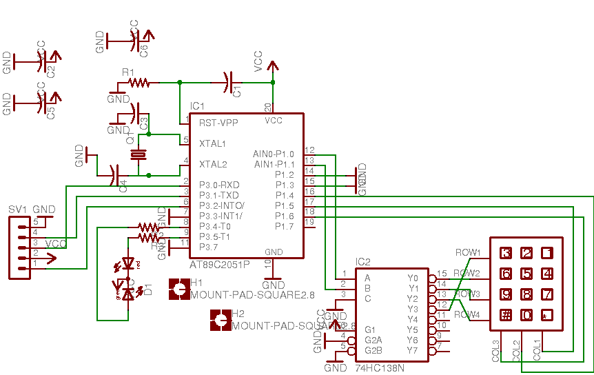
I made myself a small PCB (measuring about 6cm by 5cm). This is what is supposed to happen:
- Upon power-up, the LED goes red to indicate that the unit is ready for input.
- I then press any key down (where the contacts in the button meet), then the red led goes off.
- The correct value is found from a memory location that is determined based on the row and column the key press is detected.
- The program waits until the remote unit bit-bangs 4 bits out so that it knows the button that's pressed.
- The green light goes off and no lights are on until no key is pressed in the current row for 30+ms.
- The red light goes back on and the entire process repeats.
The problem is sometimes I can't get past step 2. It seems that with my current setup, only keys are detected from one row only. Adding a delay of 128+uS before changing the row does help somewhat (it allows me to detect 9 keys instead of 3), but I can't seem to detect the last two keys in the last row of keys no matter what I do.
I made sure all my hardware is connected correctly, and I made sure all input ports stay as inputs so that nothing blows up in my face.
This is the datasheet to my keypad:
http://futurlec.com/Keypad3x4.shtml
Here's the code:
;Keypad uC version

;Microcontroller Uses 22.1184Mhz crystal

;LED indicators. low value = LED on
RED equ P3.4
GREEN equ P3.5

;Serial Data connection
DAT equ P3.0  ;Data
CLKO equ P3.2 ;Clock out to parent uC
CLKI equ P3.1 ;Clock ack from parent uC

org 0h
mov IE,#0h ;Clear automatic interrupts so program doesn't act funny
mov P3,#0FFh ;Set IO lines to high-impedance
mov P1,#0FFh

;49h to 7Ch = number matrix space
;These values are returned for corresponding number. Will explain later...
;Note: Value 0Ah = star and Value 0Bh = pound
mov 01001100b,#06h
mov 01001010b,#04h
mov 01001001b,#05h
mov 01011100b,#09h
mov 01011010b,#07h
mov 01011001b,#08h
mov 01101100b,#0Bh
mov 01101010b,#0Ah
mov 01101001b,#00h
mov 01111100b,#03h
mov 01111010b,#01h
mov 01111001b,#02h

premain:
clr RED ;Turn red light on to indicate we're ready for keypad input
main:
  inc R6        ;Select next row
  orl 6h,#0FCh  ;Make row range 0 - 3
  mov P1,R6     ;P1.2 to P1.7 = logic 1 to accept input. P1.0 and P1.1=row #
  nop           ;waste machine cycles to let hardware catch up
  nop
  nop
  nop
  nop
  mov A,P1      ;Scan all 3 columns at once
  anl A,#070h   ;We only want P1.6, P1.5 and P1.4 bits since columns connect there
  cjne A,#070h,detk ;See if any of the above bits are low
  sjmp main     ;here, they're all high so start over continuing with next row.
detk:

;Here a key is detected (but for some keys this is never reached. why?)

;So based on informarion, we make a memory address that contains the value we
;pressed.

setb RED         ;Turn off red light

mov B,R6         ;Copy row info to B
anl B,#03h       ;We only want LSB and bit next to it. It contains row number.
orl A,B          ;merge row number with our pressed key config value
                ;...Value here equals 0ccc00rr where c equals column and r = row
swap A           ;Swap value
anl A,#01111111b ;Make MSB=0
orl A,#01001000b ;set the 7th and 4th bit to 1
                ;... Value here equals 01rr1ccc which is OK.
mov R0,A         ;Save value as address to data
mov A,@R0        ;Load correct data to accumulator

clr GREEN        ;Turn green light on to tell master we have data
                ;... At this point We stall until data is shifted out

rrc A            ;Extract one bit into carry
mov DAT,C        ;Set it as data
clr CLKO         ;Set clock to let master know we have data
jb CLKI,$        ;Wait until master acknowledges this

rrc A            ;Do same but use raised clock lines here
mov DAT,C
setb CLKO
jnb CLKI,$

rrc A            ;Repeat for remaining two bits
mov DAT,C
clr CLKO
jb CLKI,$

rrc A
mov DAT,C
setb CLKO
jnb CLKI,$

setb GREEN      ;Turn off green light as we are done with data

debounce:
  mov R4,#0h      ;Prepare for 30ms debounce
  mov R5,#0h
  db2:
    mov A,P1      ;Get line value
    anl A,#070h   ;We only want key values
    cjne A,#070h,debounce ;If any key in row is down within 30ms then extend time by 30ms
  djnz R4,db2   ;Here keys are not pressed so count down one register
  djnz R5,db2   ;and the other register too
sjmp premain    ;here, the keys have been let go long enough so press is valid. Start all over.
Here's the circuit:
What am I doing wrong?

