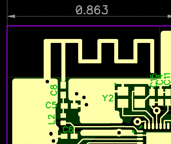
Yes, but the photo is of an "Inverted F" PCB antenna. VERY different beast. Missing from the "F" photo are via stitching of the ground plane around the perimeter of the antenna element. Without via stitching, a conductor greater in length than 1/10th the wavelength will start to behave as an antenna itself, and induce voltage onto it. Also notice that the feedline necks down to a very small and thin point right after C8 - this could be a drawing error and may cause problems.
Anyways, for a copper spring antenna, just like the F antenna, every aspect of the physical dimensions are critical to correct operation. This includes not only the length of the spring, but it's spacing and orientation to the ground plane and any nearby metal objects. Also critical are the impedance-matching components - L and C values in series and to ground to control the impedance from source to antenna. The width of the trace leading to the antenna is critical, as width has a corresponding impedance. Every aspect of this antenna - matching component values, distances, orientations... all influence how the antenna works and how efficient it is. Get any one of them wrong, and it may not work at all.
To calculate all of this by hand would require a college degree in RF engineering. Usually much easier, is to find a reference design using this antenna (at 868MHz; everything must be the same) and modify it to physically fit into your design. Ground planes can usually be extended without much influence to operation, so stick it in the corner of your PCB.
Even so, the matching component values may benefit from slight adjustment in your finished product. Usually this is determined by measuring antenna performance using a VNA to obtain the s-parameters. This indicates the efficiency and what component(s) need changed and by how much.

