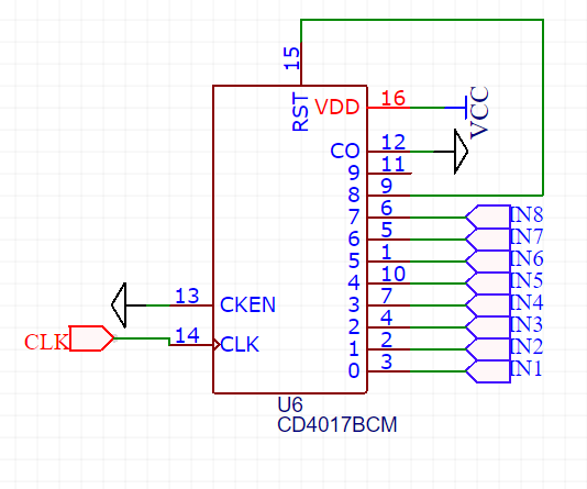
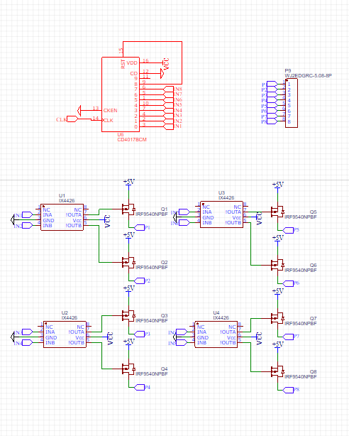
I'm using a CD4017 to control 8 Mosfets. But my problem is that I only get a output from just 1 pin, this pin is random every time i power up the ic. I wired it up like that  I shorted reset and output 8 to reset the ic and restart with 0. Is that the mistake or do I have a thinking error?
\$\begingroup\$
\$\endgroup\$
5
-
\$\begingroup\$ What is the value of the VCC voltage? \$\endgroup\$– crj11Commented Sep 6, 2018 at 16:40
-
1\$\begingroup\$ Have you verified that the clock is toggling? \$\endgroup\$– crj11Commented Sep 6, 2018 at 16:45
-
3\$\begingroup\$ The 'CO' pin is an output. Don't ground it. \$\endgroup\$– brhansCommented Sep 6, 2018 at 16:55
-
\$\begingroup\$ @crj11 vcc is 12V, yes the clock should toggle, i just checked it with a multimeter and arduino. \$\endgroup\$– RibislCommented Sep 6, 2018 at 17:32
-
1\$\begingroup\$ Random starting output always seems to be a reset problem. First, I would try just groud reset (pin 15), and let output 8 (pin 9) and output 9 (pin 11) floating. See if this works (there will be a delay after output 7 turning off, before output 0 turns on). If this works, you should put a pull-down to reset pin; maybe the initial state of pin 8 is not enough to trigger reset. \$\endgroup\$– mguimaCommented Sep 6, 2018 at 18:09
Add a comment
|
1 Answer
\$\begingroup\$
\$\endgroup\$
2
You have a few problems.
- CKEN should be labelled CK_INH. When high it INHibits the clock rather than ENabling it. It is, however, wired correctly.
- CO is the Carry Out output pin. It turns on for outputs 0 to 4 and off for outputs 5 to 9. It should not be short-circuited to ground. This may be responsible for some of your troubles.
- On power-up the counter will assume a random state unless you do a power-up reset.
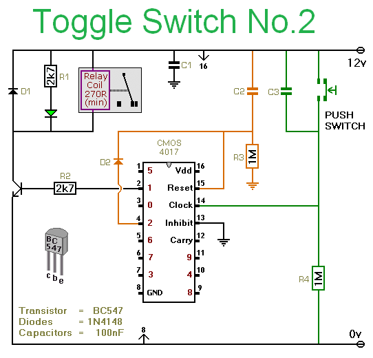
Figure 1. A divide by two implementation with a power-up reset. Source: Zen.
How it works:
- On power-up C2 is discharged so when the supply ramps up from 0 V to 12 V the bottom of C2 does too. This applies the reset to pin 15. Output 0 will turn on.
- R3 charges C2 (by pulling the bottom terminal to ground). The reset pulse time period can be calculated from \$ \tau = RC \$. When the RST voltage falls to about 1/2 or 1/3 of Vdd the reset will be released and the chip will respond to clock pulses.
- In this application output 2 is wired via a diode to C2 / R3 so every time it goes high the chip is reset to zero. (You will be using output 8.) Note that the chip won't respond to clock pulses again until the reset signal falls low again. For this reason your \$ \tau \$ needs to be shorter than your fastest clock period.
-
\$\begingroup\$ @Dave Tweed - I question a design that is likely to blow up the CD4017 outputs when the MOSFET turns on and shorts 5V to an output trying to pull low, and you delete my post? That seems pretty unhelpful dude. \$\endgroup\$ Commented Sep 6, 2018 at 23:45
-
\$\begingroup\$ I would guess that Dave read it as someone asking a question instead of posting an answer. I've given it a 'reopen' vote. Note that putting your comment in my answer isn't the right place as it has nothing to do with me. \$\endgroup\$ Commented Sep 7, 2018 at 6:40


