2
\$\begingroup\$

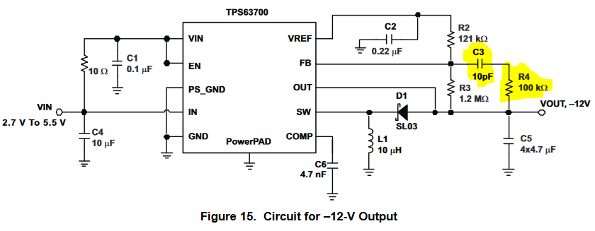
I was looking at the TPS63700 DC-DC inverter datasheet and stumbled across the schematic below. It is a more or less usual buck-boost inverter topology schematic, except for the weird R4 and C3 components. I haven't got much experience in SMPS design, however, I've never seen a feedback loop with these components. The datasheet says that

To speed up the control loop, a feed-forward capacitor of 10 pF is recommended in the feedback divider, parallel to R3. To avoid coupling noise into the control loop from the feed-forward capacitor, the feed-forward effect can be bandwidth-limited by adding series resistor R4. A value in the range of 100 kΩ is suitable. The higher the resistance, the lower the noise coupled into the control loop system.

So, my questions:

  • What exactly do they mean by "speeding up" the control loop and why or how does it enhance the performance?
  • Except for the mentioned induced noise in the feedback circuit, are there any other drawbacks of using this schematic?
  • In which SMPS topologies can this feedback quirk be used (especially in high-order ones like SEPIC, Cuk, etc.)?
  • Should this feedback quirk be used with other ICs and if not - why?

TPS63700 datasheet link: http://www.ti.com/lit/ds/symlink/tps63700.pdf

Recommended schematic from the TPS63700 datasheet

\$\endgroup\$

2 Answers 2

1
\$\begingroup\$

The Ron of this TPSxxx Out and 4x C5 loads form a LPF with a 90 loss in phase margin with the benefit of Zout reducing with rising f while attenuating f(PWM).

To improve current step response overshoot which is a function of phase margin, those RC added increase the loop gain by a factor of 10, while differentiating over 2 decades of leading phase shift centred at 45 deg @ 2pifC=1/R.

This can improve phase margin and transient error in step changes in input or output.

This a classic “lead-lag” compensation filter common to many Control Systems. I have used it 40 yrs ago in CMOS PLL Loop filters to improve speed and stability.

The purpose is to reduce full step transient error overshoot in a 2nd Order system with a trade off on noise. Full details can be found in any Control System textbook.

The datasheet simply says:

8.2.2.3 Stabilizing the Control Loop

8.2.2.3.1 Feedback Divider To speed up the control loop, a feed-forward capacitor of 10 pF is recommended in the feedback divider, parallel to R3. To avoid coupling noise into the control loop from the feed-forward capacitor, the feed-forward effect can be bandwidth-limited by adding series resistor R4. A value in the range of 100 kΩ is suitable. The higher the resistance, the lower the noise coupled into the control loop system.

——- I.e. Stability, Speed, without excess noise gain.

You should read to understand what these mean.

overshoot, ringing

step response, Load current rise/fall time (faster error reduction)

Bottom line is demand current is not met, there is an error voltage at the event start until settling is complete . This is added to the expected ripple voltage and is part of every power supply. Spec.

\$\endgroup\$
2
  • \$\begingroup\$ "The purpose is to reduce full step transient error overshoot in a 2nd Order system" - so it can't be used with a 4th order like SEPIC? \$\endgroup\$
    – sx107
    Commented Oct 15, 2018 at 8:02
  • \$\begingroup\$ If you have any high order control system, then you use Nyquist dominant root analysis near RHP for designing a filter I would think, but this could be used for many systems , again trade off for improved stability and rise time is less noise reduction.. \$\endgroup\$
    – D.A.S.
    Commented Oct 15, 2018 at 12:20
2
\$\begingroup\$

At start-up, or during any high-frequency transient, the capacitor will effectively be a short-circuit. This means the feedback voltage divider will look like this:

schematic

simulate this circuit – Schematic created using CircuitLab

Because of this, the feedback pin voltage will be a lot higher (with respect to VREF) than it would be without the C3 and R4. This higher voltage means there will be a higher error, which means the control system regulating the output voltage will ramp harder towards the correct voltage, to achieve stabilisation. As it tends towards this, the capacitor will slowly become higher and higher impedance, and eventually the C3/R4 combination will be an open-circuit, and essentially not even there at steady-state.

The only draw back is the potential for instability if you choose incorrect values. Every component at every part inside a SMPS circuit affects the transfer function, and therefore can effect how the device performs.

This method of having a faster-response to transient/start-up can be used on anything that has some sort of feedback mechanism with a voltage divider.

The reason you don't see it everywhere? Well, it's not really needed. The system will stabilise eventually with or without it. It's just a nice feature to improve high-speed performance.

\$\endgroup\$
1
  • \$\begingroup\$ The stability is improved, not a drawback. The only drawback is a gain in ripple noise. \$\endgroup\$
    – D.A.S.
    Commented Oct 15, 2018 at 1:57

Your Answer

By clicking “Post Your Answer”, you agree to our terms of service and acknowledge you have read our privacy policy.

Not the answer you're looking for? Browse other questions tagged or ask your own question.