1
\$\begingroup\$

Say I am running my 74LVC125 at 2.5V. At the A input I have a logic 1 and at the nOE input, I have a logic 0, so the device should be driving a logic 1 onto the Y output.

With no load connected to the Y output, I should observe 2.5V at the output, obviously.

Now say I have a load along the lines of 1kohm to 5V. What happens? I choose 74LVC125 for my example because for tristate LVC logic, in the high-Z state (nOE high), applying higher voltage than Vcc on an output is allowed. But what about with the output enabled?

  • Will it sink something like (5.0V - 2.5V) / 1kOhm = 2.5mA?
  • Will very little current flow?
  • Will it sink more current than I would expect? The TVS diodes of the LVC device will not yet flow current, but will some kind of reverse bias damage happen to the rest of the LVC driver IC?

I want the first thing to happen, that is for the 'LVC125 to sink something like 2.5mA into 2.5V. Using a logic circuit like 74LVC125 is cheaper and than applying several MOSFETs for this purpose. Can it be done?

\$\endgroup\$
1
  • \$\begingroup\$ Most devices with open-drain outputs (e.g., '07) are designed to allow higher output voltages. \$\endgroup\$
    – CL.
    Commented Nov 16, 2018 at 20:40

2 Answers 2

2
\$\begingroup\$

It is not allowed, according to the datasheet, to apply any more than Vcc + 0.5V (absolute maximum) to the output.

enter image description here

However the built in clamp diodes can withstand a certain amount of current (not specified, but below GND -50mA is permitted.

So with the output high-Z and a pullup to +5 the output will be about at the Vcc rail + 0.7V (or ~5V, whichever is less). The Vcc rail may well not stay at 2.5V and may be pulled up to approaching 5V depending on what else is on the rail, since most voltage regulators will not sink current.

With the output enabled and high, the high-side MOSFET (p-channel) will be "on' and conducting (in reverse) and the above sentence also applies, however there will no longer be a diode drop involved.

\$\endgroup\$
1
\$\begingroup\$

I know this question is quite old and your design has be finalized long ago but I think this is very part specific. The TI part mentioned above does indeed seem to cap out at VCC + 0.5V but the Nexperia part specifically calls out a 3-state output max of 6.5V:

74LVC125 datasheet output maximums

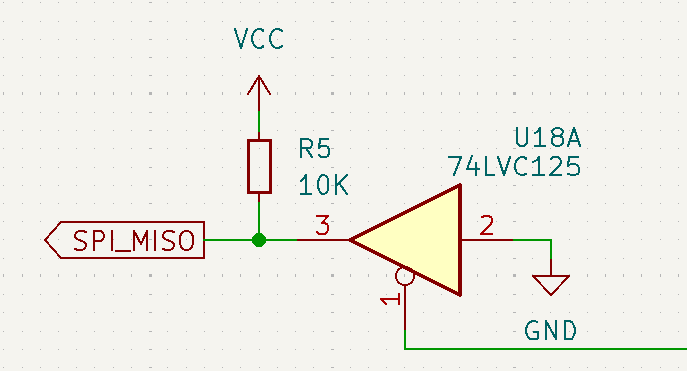
So I believe it's possible to translate a 3.3V input to 5V output by connecting input to ground, your real input to /OE, and pull output up to 5V via resistor:

schematic using 74LVC125

When your input is a 1, the buffer will be high Z and get pulled up to 5v on the output. When your input is a 0, buffer will turn on and get driven low. But this looks like it's only valid with the Nexperia part!

\$\endgroup\$
1
  • \$\begingroup\$ That's a very good point! It seems like the situation with output voltage tolerance is very confusing with the LVC series... While TI's 74LVC125 doesn't tolerate output overvoltage, their 74LVC1G125 does allow up to 6.5V in the high-Z state. The Diotec 1G125 also allows it. But now, hold onto your hats: While the Nexperia '125 allows 6.5V in high-Z, their '1G125 does not, so they're exactly the opposite of TI! ARGH!! \$\endgroup\$ Commented Nov 15 at 9:16

Your Answer

By clicking “Post Your Answer”, you agree to our terms of service and acknowledge you have read our privacy policy.

Not the answer you're looking for? Browse other questions tagged or ask your own question.