2
\$\begingroup\$

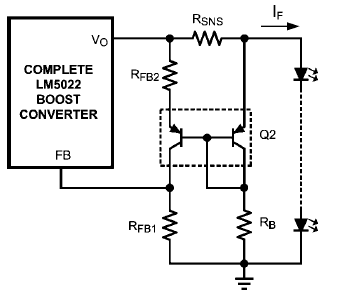
I came across this circuit for a high-side current sense using BJT current mirror, and I am trying to derive a formula for how I could calculate the sense voltage output (going to the FB pin) in terms of Isense and the resistors used. I am having a hard time understanding how they derived their formulas. Firstly where does the 1.25 come from to calculate their \$R_\mathrm{FB1}\$, and when it says suggested bias current of 1mA, is this talking about base current, and why 1mA?

Current Sense amplifier

Resistor \$R_\mathrm{B}\$ sets a bias current through the right-hand transistor. The suggested bias current for the PNP transistors is 1 mA. \$R_\mathrm{B}\$ is selected by dividing the typical output voltage minus one diode drop by 1 mA. $$ R_\mathrm{B} = \frac{V_\mathrm{O} – 0.6}{0.001} = 32.6\mathrm{k}\Omega\label{1}\tag{5} $$ $$ R_\mathrm{B} = 32.4\mathrm{k}\Omega\pm 1\% \label{2}\tag{6} $$ \$R_\mathrm{FB1}\$ is set to bias the left-hand PNP at 1 mA, using the following expression $$ R_\mathrm{FB1} = {1.25 \over 0.001} = 1.25\mathrm{k}\Omega \label{3}\tag{7} $$ $$ R_\mathrm{FB1} = 1.24 \mathrm{k}\Omega\pm 1\% \label{4}\tag{8} $$ \$R_\mathrm{FB2}\$ is set to amplify the current sense signal to equal the feedback voltage: $$ R_\mathrm{FB2} = \frac{I_\mathrm{F} \times R_\mathrm{SNS} \times R_\mathrm{FB1}}{1.25} \label{5}\tag{9} $$ $$ R_\mathrm{FB2} = \frac{1.0 \times 0.2 \times 1240}{1.25} = 198\Omega \label{6}\tag{10} $$ $$ R_\mathrm{FB2}\text{ is }200\Omega\pm 1\% \label{7}\tag{11} $$ Texas Instruments Application Note: AN-1696

Now using "1" for left transistor and "2" for right transistor:

From my understanding the base of the two transistors will be at \$V_\mathrm{O} - V_\mathrm{BE2}\$ (forward drop of right-hand transistor). Doing KVL around the top loop, you have $$ R_\mathrm{SNS}\cdot I_\mathrm{SNS} + V_{BE2} = V_{BE1} + R_\mathrm{FB2}\cdot I_{E1}. $$ For a matched pair, where \$V_\mathrm{BE1} \sim V_\mathrm{BE2}\$, this gives $$ R_\mathrm{SNS}\cdot I_\mathrm{SNS} = R_\mathrm{FB2}\cdot I_{E1}, $$ so \$R_\mathrm{FB2}\$ has the same potential across it as \$R_\mathrm{SNS}\$, and for a given sense resistor and load current, \$I_\mathrm{E1}\$ is set by \$R_\mathrm{FB2}\$ as: $$ I_\mathrm{E1} = \frac{R_\mathrm{SNS}\cdot I_\mathrm{SNS}}{R_\mathrm{FB2}}. $$ Since \$I_\mathrm{E1} \gg I_\mathrm{B1}\$, then \$I_\mathrm{C1} \sim I_\mathrm{E1}\$, so \$V_\mathrm{SNS}\sim I_\mathrm{E1}\cdot R_\mathrm{FB2}\$. So: $$ V_\mathrm{SNS} = R_\mathrm{SNS}\cdot I_\mathrm{SNS}\cdot\frac{R_\mathrm{FB1}}{R_\mathrm{FB2}}. $$

So is this a correct formula to use for the \$V_\mathrm{SNS}\$ output?

I think I'm not understanding something correctly, because I don't get what effect \$R_\mathrm{B}\$ actually has on this formula? The formula I derived above does not include \$R_\mathrm{B}\$, but I think the base current of both transistors is set by \$R_\mathrm{B}\$, and the collector/emitter current should be related to base current as an approximation: $$ I_\mathrm{B} = \frac{I_\mathrm{E}}{\beta}, $$ where \$\beta\$ is the current gain - but if I try to derive a formula that way I can't seem to get the same result.

So where should base current and \$\beta\$ come into these calculations?

Could you not just replace the transistor pair (emitter diodes) with two regular diodes OR'd together and connected to \$R_\mathrm{FB1}\$, and arrive at the same formula, and functionality?

\$\endgroup\$
2
  • \$\begingroup\$ 1.25 V is probably the internal reference voltage. It's a very common reference voltage due to being easy to obtain with a low temperature coefficient using a Brokaw bandgap reference circuit. \$\endgroup\$
    – Hearth
    Commented Dec 2, 2018 at 17:58
  • \$\begingroup\$ \$\nabla_x\$: \$R_\text{B}\$ sets the quiescent current for the mirror. This current does affect some of the calculations, but not in any important way in their case. But, for example, their computation of \$R_{\text{FB}_2}\$ doesn't mathematically pencil out right. But it is "close enough" for electronic design. The actual computation should be: \$R_{\text{FB}_2}=R_\text{SNS}\cdot\left(\frac{I_F}{I_Q}+1\right)\$, where \$I_Q=\frac{1.25\:\text{V}}{R_{\text{FB}_1}}\$ and not the equation they provide. But theirs is close enough, since the +1 part doesn't count for much in their context. \$\endgroup\$
    – jonk
    Commented Dec 2, 2018 at 18:54

3 Answers 3

2
\$\begingroup\$

hFE or Beta does not affect this design which is like an H biased common emitter.

The voltage drop across Rsns is compared with an internal 1.25V bandgap reference for linear current regulation.

The gain is controlled by Rc/Re = Rfb1/Rfb2 = Av = 1240/200 = 6.2 or 1.25k/200 =0.125. I see they chose 1240 as the nearest value.

The Rsns in your question appears to be 0.2 ohms or 0.2V/A for an input current to voltage conversion.

Thus the gain is chosen to equal 1.25V ( just like in LM317's on Vadj to Vout drop is always 1.25V)

6.25*0.2V/A = 1.25V @ 1A but since they chose 1240 instead of 1.25k

6.2 * 0.2V/A = 1.24V so to achieve 1.25V in the high gain comparator feedback loop, the current must increase from 1A to 1.008A so the drop voltage on Rsns= goes from 0.2 to 0.2016V.

more details

This is <1% and R tolerances will contribute some errors in addition to rounding error of choose nearest R values.

A good designer works SPECS for Isns and % Tolerance to choose the final component values.

Unlike an LM317 used as a Current Limiter which drops 1.25V minimum for Vadj and more for headroom on Vin, this design only drops 0.2V/A. When you compute the power dissipation at 1A it is 0.2W which means for a 1/4W resistor rated for a 125'C temperature @ 25'C , that part will reach 0.2/0.25 80% of the 100'C temperature rise which will burn your finger unless you choose a 1/2W or more R.

There's a good chance of burning fingers on your LEDs too with 1A * 3V unless you compute your thermal resistance of the design Tja [W/'C]

A better design always uses a smaller voltage drop for current shunts and this is why 50mV to 75mV is pretty standard but then your input offset voltage becomes more critical but that can be solved..

The regulation heat loss must be dumped somewhere, so using a higher power Resistor is better than heating up the linear regulator. so to avoid both heat loss, PWM designs such as this often use a hysteresis mode with an inductor to store the energy. Now you have an efficient SMPS current regulator with the LM5022. I'll let you figure out how the rest works with hysteresis and a LPF for current sense filter to COMP input.

\$\endgroup\$
1
\$\begingroup\$

As with anything in engineering it is all about doing the right approximations, so as to simplify the required equations and prime our intuition. .

You can see the circuit in several different ways, all of which would be correct to one degree or another. All of which can bring some insight on the working of the circuit.

  1. As a slightly modified Widlar current source, that requires solving a transcendental equation.
  2. As a common-base differential amplifier with \$I_FR_{SNS}\$ as its own input, \$~V_{OUT}\$ as the bias/common mode voltage, and RB and \$R_{FB2}\$ as the feedback network.
  3. As a common-base amplifier biased by a diode-connected transistor and With \$R_{FB2}\$ as feedback.
  4. As a common emitter amplifier. With \$R_{FB2}/R_{FB1}\$ as a good approximation to its gain.
  5. As individual transistors solving approximate KCL equations.
  6. Use all of the above and examine the limit conditions.

As a Widlar current source, you know that the current on the Q2 branch will define the mirror bias and, depending on \$R_{SNS}\$ and the output current, will be higher than the current through the Q1 branch. You are designing for \$V_{OUT}\$, you know the sense resistor drop will be small, so you choose a reasonable bias for the mirror and choice of transistors. 1mA is a reasonable bias in many cases, so would be 0.1mA, and 10mA seems wasteful. This choice mostly affects the frequency response of the amplifier which could interact with the regulator feedback loop and affect stability.

But here is where your analysis gets into trouble. You assume that Vbe of both transistors has to be the same, which automatically forces their currents to be the same, which also goes against what we know about that type of current mirror.

The reason TI assumes 1.25V across \$R_{FB1}\$ With 1mA in it, is because this is the desired bias condition and that is the voltage imposed by the feedback loop of the regulator. The only way this can happen is if the drop across RFB2 and RSNS is the same.

So the ratio \$R_{FB2}/R_{SNS}\$ multiplied by the bias current of 1mA determines the design’s output current.

So. What happens if there is no load? The output voltage will increase until 1mA goes through RFB1. This will require a large current on RB, as determined by the Widlar mirror. So RB and RFB2 determine the maximum output voltage (figuring it out requires solving the transcendental equation).

But more to the point, \$R_{B}/R_{FB1} * 1.25V + 0.7V\$ determines the output voltage at the desired operating condition.

Do note that there is a balancing act. Both Vout and IF are being regulated by the feedback loop. But the gain for the current is \$R_{SNS} * R_{FB2}/R_{FB1}\$ while for the voltage is \$R_B /R_{FB1}\$

\$\endgroup\$
0
\$\begingroup\$

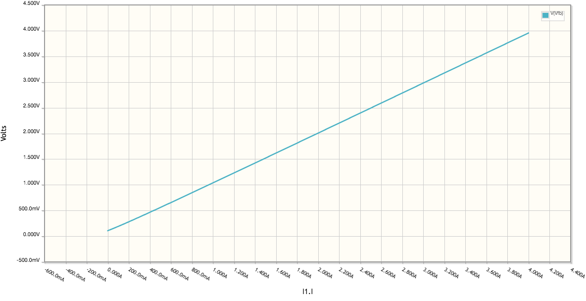
This circuit is quite linear, but lacks accuracy when the voltage across Rsense is too low.

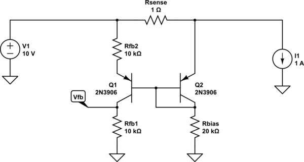
schematic

Here is a simulation showing Vfb as a I1 varies.

enter image description here

How it works

The bases of the Q1 and Q2 are tied together. If the base-emitter voltages are equal, then the emitters of Q1 and Q2 will be at the same voltage. This will cause the voltages across \$R_{sense}\$ and \$R_{fb2}\$ to be equal, and the ratio of currents through those two resistor will be the same as the ratio of their conductances.

$$\frac{I_{Rfb2}}{I_{Rsense}} = \frac{R_{sense}}{R_{fb2}}$$

If we neglect the base current of Q1, and any current flowing out of the \$V_{fb}\$ connection, the current through \$R_{fb2}\$ will equal the current through \$R_{fb1}\$.

Therefore the voltage at \$V_{fb}\$ will ideally be given by

$$V_{fb} = R_{fb1}\frac{R_{sense}}{R_{fb2}}I_{Rsense}$$

In many cases, this formula is good enough and we can neglect the 2nd order effects due to base currents currents and to the Vfb output as well as differences in \$V_{be}\$. However, when the voltage across \$R_{sense}\$ is small, the percentage error in the output is significant.

\$\endgroup\$

Your Answer

By clicking “Post Your Answer”, you agree to our terms of service and acknowledge you have read our privacy policy.

Not the answer you're looking for? Browse other questions tagged or ask your own question.