0
\$\begingroup\$

I came across instances where NMOS was used as a capacitor in analog circuits. This is done by shorting the drain and source. The drain/source acts as one terminal of the capacitor while gate acts as the other terminal, as shown below. enter image description here Here are some observations about its working:
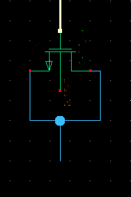
1) This acts like a capacitor if drain/source terminal is connected to ground. If drain/source is connected to VDD, its as good as open (0 capacitance) 2) To get a good capacitance value when drain/source is grounded, we have to use a large length and small width for the NMOS

Now, I am trying to reason out these observations.

1) I guess that when drain/source is grounded, the gate oxide acts like the capacitor with n-doped regions providing the charges. But what happens when drain/source is set to VDD. Why can't it still act like a capacitor between gate and the body?

2) How to reason out the need for large length and small width? I guess it is to reduce the effect of overlap caps between the gate and drain/source. But I am not able to arrive at a good explanation.

\$\endgroup\$

1 Answer 1

1
\$\begingroup\$

If drain/source is connected to VDD, its as good as open (0 capacitance)

That is not true, you get less capacitance but not zero.

How to reason out the need for large length and small width?

Also a wrong assumption, any size of MOSFET will work as a capacitor. The series resistance of the capacitor is generally smaller (you get a "better" capacitor) when the width is large and length is small. But in practice I usually make these MOS capacitors (somewhat) square as that is a good compromise between series resistance and capacitance per area.

\$\endgroup\$
3
  • \$\begingroup\$ Some semiconductor processes allow the layout to have "capacitor" labels placed on the FETS; during processing, those FETs will have the region between Source-and--Drain altered with extra doping, and the threshold voltage is shifted away from normal values; this shifted-Vthreshold gives a more-constant gate-bulk (gate-tub, gate-well) V_C curve. \$\endgroup\$ Commented Feb 1, 2019 at 14:51
  • \$\begingroup\$ Thanks for the reply Bimpelrekkie and analogsystemsrf. But I'm not able to visualise clearly how length and width relate to the series resistance as well as the capacitance ( for instance which has higher capacitance, nmos with larger length or one with larger width) \$\endgroup\$ Commented Feb 2, 2019 at 15:12
  • \$\begingroup\$ The capacitance is mostly related to the gate area of the MOSFET, so width x length. Series resistance is more complex, the silicon substrate has some resistance so if you contact it with a larger area (long drains and sources meaning a wide MOSFET) then series resistance becomes smaller. \$\endgroup\$ Commented Feb 2, 2019 at 17:18

Your Answer

By clicking “Post Your Answer”, you agree to our terms of service and acknowledge you have read our privacy policy.

Not the answer you're looking for? Browse other questions tagged or ask your own question.