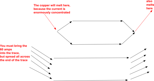
The current in my circuit is 60A and voltage is 36V. How wide should the tracks on my PCB be?
-
\$\begingroup\$ I am not sure about Proteus, but there are numerous online calculators. PS 60 amp track will be super wide! \$\endgroup\$– TylerCommented Mar 3, 2019 at 15:01
-
\$\begingroup\$ For traces on 2 oz copper board at 10 degree temperature rise from 25 degrees ambient, you'll want 111mm wide internal traces and 42.6 mm wide external traces. For 4 oz copper board, half that. Perhaps consider using wires instead. \$\endgroup\$– K HCommented Mar 4, 2019 at 4:29
3 Answers
You'll need it wide, and thick if you can (2 oz copper vs 1 oz copper). There are calculators like this one https://www.4pcb.com/trace-width-calculator.html that take into account current, copper thickness, allowed heat rise, internal or external trace, trace length into account and calculate a trace width. Other board houses have calculators also.
This is not determined by board houses or PCB design software, but by IPC standards. IPC-2221A Section 6.2 states:
The minimum width and thickness of conductors on the finished board shall be determined primarily on the basis of the current-carrying capacity required, and the maximum permissible conductor temperature rise.
The formula provided in the standard is:
$$ I=k\Delta T^{0.44}A^{0.725} $$
where:
- \$I\$ is the current handling requirement in amperes
- \$\Delta T\$ is the allowed temperature rise of the trace in degrees Celsius
- \$A\$ is the the cross-sectional area of the trace in square mils
- \$k\$ is a constant which equals 0.048 for outer layer traces, or 0.024 for inner layer traces.
The cross-sectional area is determined by your trace width and your copper weight (measured in mils, millimeters, or oz/ft^2). If you don't want to do the math by hand, there are certainly plenty of calculators out there on the net. My point is that it is not a custom value depending on your board house, your design software, or anything of that sort. They will all point to this formula, so I simply prefer to skip the middle man and calculate the required trace widths myself from the start.
-
\$\begingroup\$ That formula does not depend on trace length, but a long trace will get hotter than a very short one. \$\endgroup\$– UweCommented Mar 4, 2019 at 20:44
-
\$\begingroup\$ @Uwe Source? You may be right, but the formula used above is what is called out in what can be considered THE bible of PCB design. \$\endgroup\$ Commented Mar 4, 2019 at 22:12
-
\$\begingroup\$ If it is a good bible of PCB design, there should be some sentences about the conditions when this formula is applicable. A large PCB filled with a high current coil with many windings would get much hotter than calculated. \$\endgroup\$– UweCommented Mar 5, 2019 at 11:04

