Scenario
I have a motherboard and a daughterboard that couple through two headers.
The motherboard has a 16x16 array of ultrasound speakers each with their own drivers, that works. I drive them using 32 74HC595D shift registers. That works too.
The daughterboard houses various power electronics, control electronics and the FPGA carrier, featuring an Altera Cyclone IV. The signals to the motherboard include 32 serial data signals to each shift register from 32 individual GPIO pins, and RCK and SCK both being carried by a single GPIO to all shift registers.
The Problem
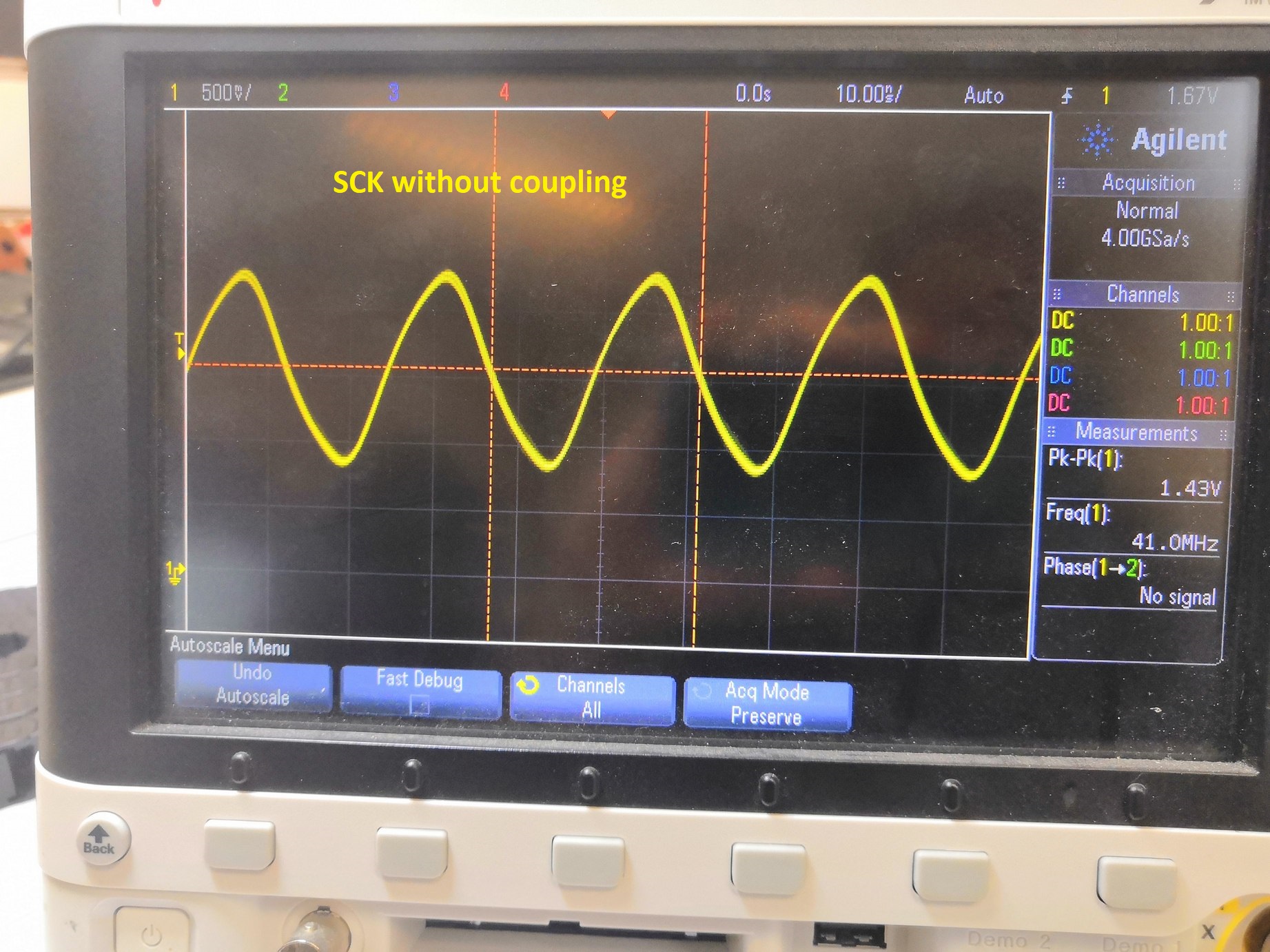
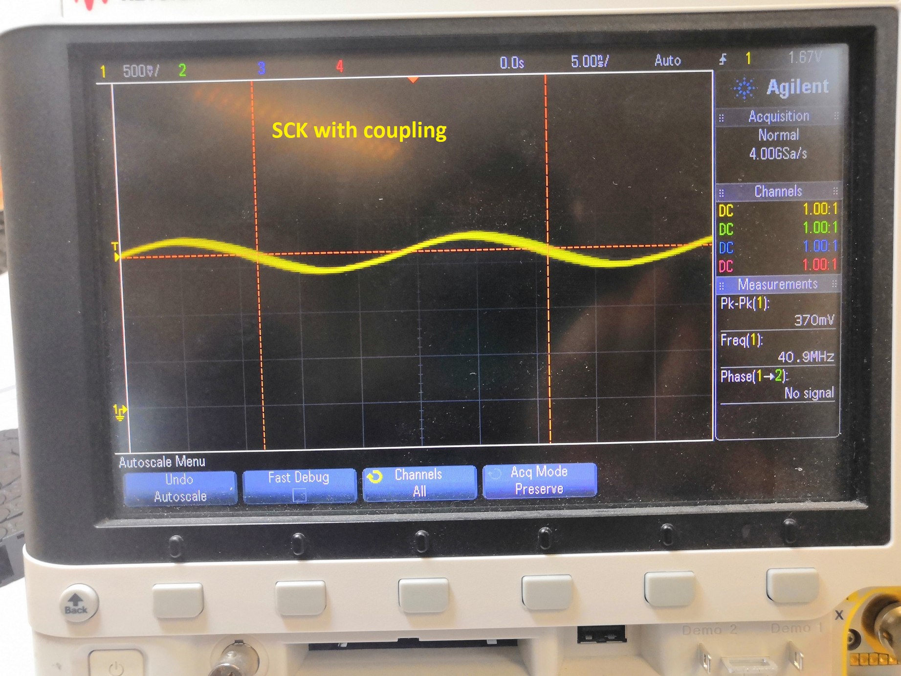
I want a clock frequency on SCK of 40MHz (I know the shift registers are happy with this), but at the moment I am limited to 20MHz on my new PCB, as the high peaks at 40MHz are below the 'High level input voltage' of the shift registers (Page 8). This is no doubt because of my retrospectively poor design choice for routing both RCK and SCK. I think this is the case in particular as when the daughter board isn't mated with the motherboard (which houses the long clock tracks) the 'square' wave has higher amplitudes.
I would like to hear opinions and advice from the stack exchange wizards on how to alleviate said issues.
The image below shows 40MHz on SCK without coupling, so it's just the FPGA's GPIO carrying 40MHz to a 2.54mm header pin. Even without coupling the amplitude is half what it should be (3V3). It's worth noting that on the daughterboard, the signal for SCK from the FPGA to the header pin does go through a test point with a via straight through the middle of the track, of which the width is 0.75 - 1mm, I wouldn't have thought the via in the track would be such an issue.
I have yet to measure the frequency with the FPGA carrier board disconnected so none of my design is touching the signal. I plan on doing this very soon.
The following image shows the 40MHz SCK signal (probed on the daughter board) when the two PCBs are coupled together. Note the daughter board has long (not daisy chained) tracks for the SCK signal.
Worth showing my retrospectively silly choice in laying out the track. Note this is only the top layer; it's a six layer board and the other layers carry very short tracks to the 32 pads, and are internal hence un-modifiable so I won't include screenshots of them. The driving signal from the header comes from the two Headers pins in the middle of the board.
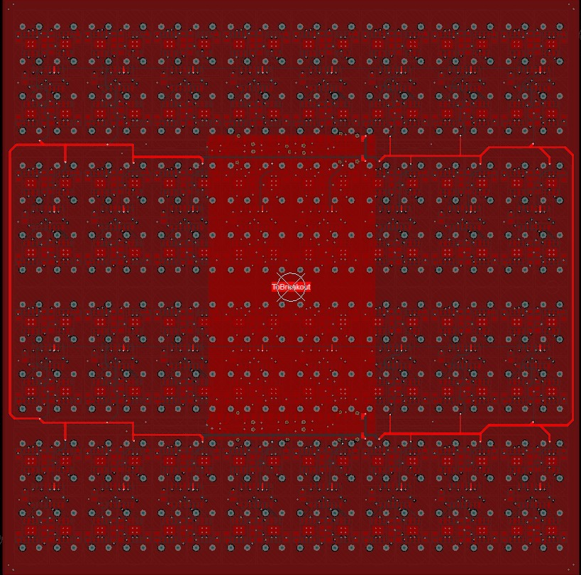
SCK on the daughter board is routed like so:

Possible Issue
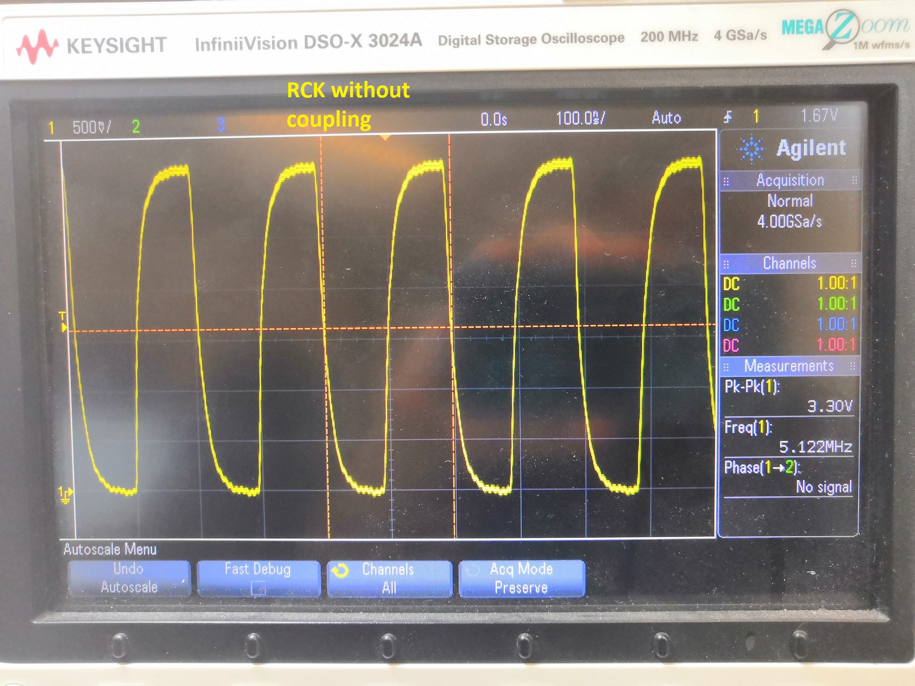
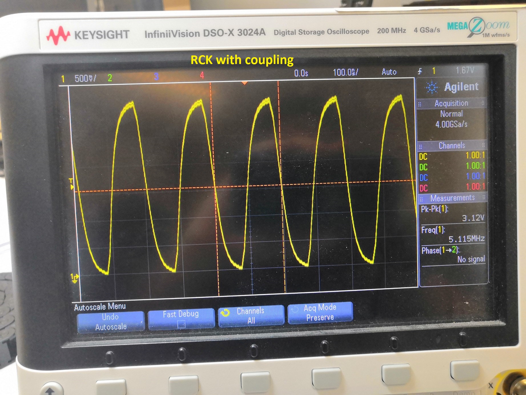
The long track on the top layer highlighted above is most likely the cause especially when you take into account the fact that the motherboard is 20x20cm. I can't see it being anything else. It's worth noting that i have a less sever issue on RCK ( 5MHz), as the High voltages are greater than 3V. Images below for reference. Note i plan on implementing whatever final fix i go with to RCK too so it's less of a sine wave and more of a square wave. Note, the routing of RCK is almost identical to SCK's.
My Ideas I have two ideas that I wanted to suggest and hear feedback on before implementing, and of course would be open to hearing other suggestions - keeping in mind I plan on re-spinning the board anyway (I had one PCB fabricated to test and adjust before buying more). I do not intend to spend much more time re-designing this board, this taken into account my ideas are:
- Leave all the tracks unmodified, and set two or more FPGA GPIO's to mirror the SCK signal (so i'm not having a single FPGA pin driving these long tracks) and hope that provides enough drive from the PLL to call it a day after I add some mod wire between those new FPGA pins and th eexisting SCK pin. To Clarify, I would have for example 2 GPIO pins --> SCK on the motherboard.
- Make some modifications to the tracks on both PCBs like so to allow two different GPIOs to drive 16 shift registers each, and removing that giant vertical trace from the motherboard. (forgive the childlike writing):

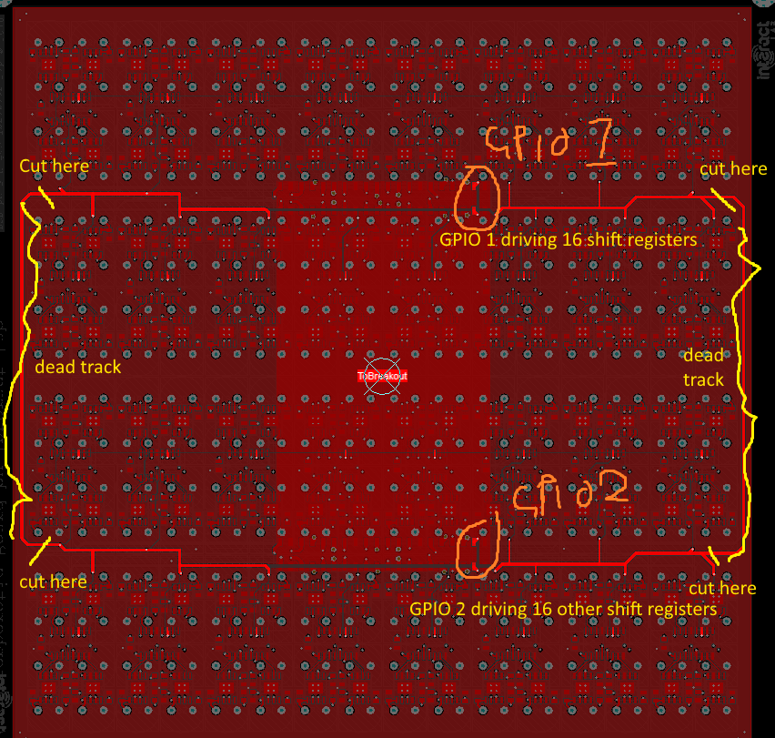
Conclusion This is for an academic research product so I am not entirely concerned about EMI, but I try to do things properly, so I would think the second solution would emit less EM interference and probably the better choice, particularly to remove the large loop(s).
I know this is a long question and appreciate any feedback and suggestions, be realistic though as this is nearing completion and a suggestion for a large re-design will not be implemented.
Thank you, and let me know if I've missed any information out.

