1
\$\begingroup\$

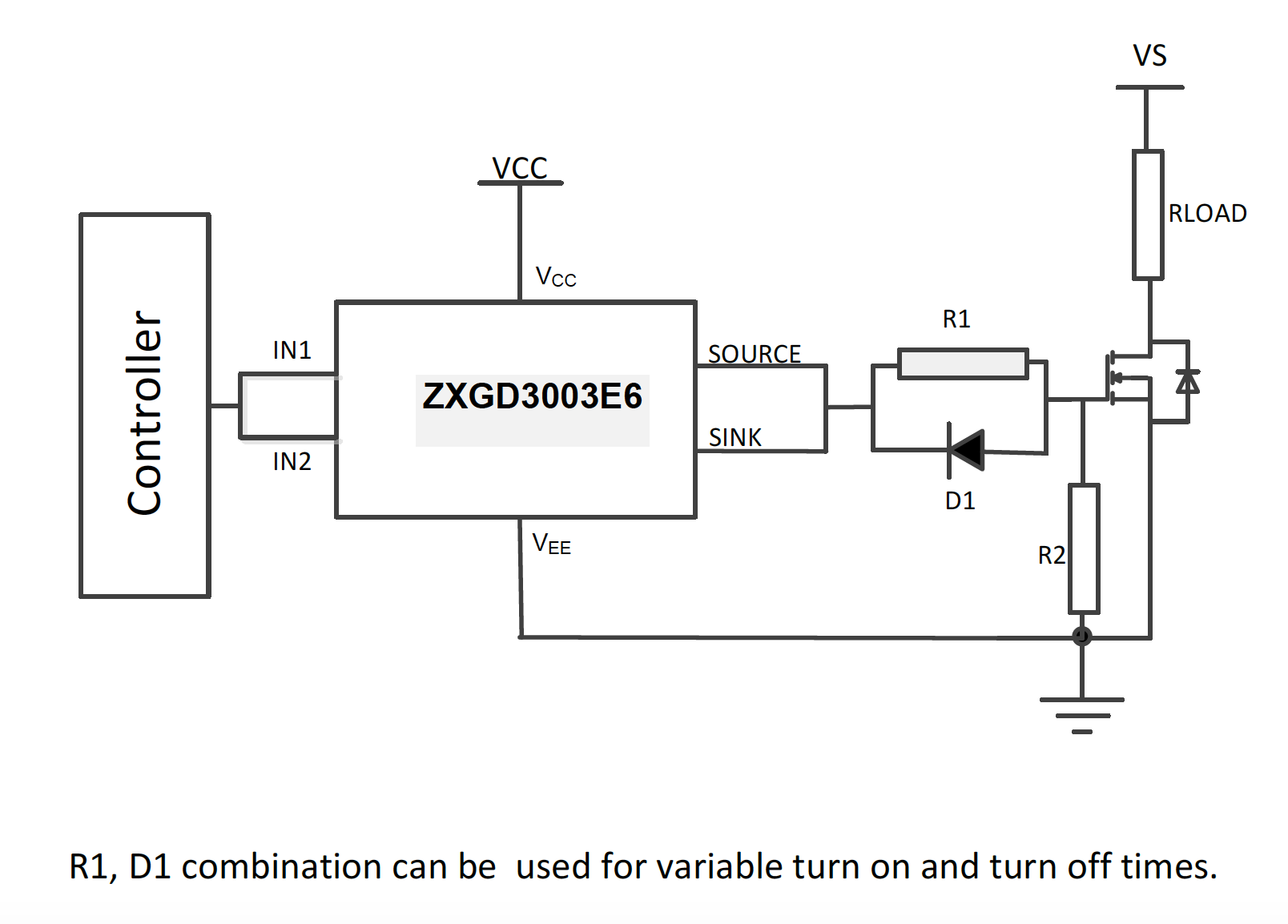
I'm considering the ZXGD3003E6 for driving an N-channel MOSFET - PSMN4R5-40PS,127. There is a typical application schematic in the MOSFET driver datasheet (as shown below). My question is how do I calculate the value of R1 and R2?

Edit: Will be driving the gate driver with a TLC272 opamp as a buffer which is connected to a 12V supply. Also the current through the MOSFET will be no more than 10A DC.

enter image description here

\$\endgroup\$
4
  • \$\begingroup\$ The values depend on what you want it to be. It's a voltage divider. However, according to the datasheet, the maximum common mode output voltage that device can withstand is ±7V. \$\endgroup\$
    – user103380
    Commented Jul 7, 2019 at 16:38
  • \$\begingroup\$ @KingDuken yes I saw that but wasn't able to understand what that meant. Could you please elaborate? \$\endgroup\$ Commented Jul 8, 2019 at 3:26
  • \$\begingroup\$ It means that whatever the difference you see at Sink and Source, it needs to be between -7 and 7. So for an example, if the voltage at Sink is 5V and Source is 2V, then the differential voltage is 3V (5-2=3). \$\endgroup\$
    – user103380
    Commented Jul 8, 2019 at 14:43
  • \$\begingroup\$ But the recommended schematic suggests that the source and sink be shorted. Which makes them at the same potential at any given point of time right? \$\endgroup\$ Commented Jul 9, 2019 at 3:35

2 Answers 2

1
\$\begingroup\$

From the driver's point of view, a power MOSFET looks like a capacitor from the gate to the source. This is why the notation says that varying the resistors changes the turn on and turn off times; those resistors work with the FET capacitance to form an R-C delay network. If you want to slow down the turn-on and turn-off voltage ramps htat the load sees at the FET drain, then R1 and R2 can do that for you. If you are just switching a relatively static load on and off, they are not needed.

Another reason for R1 is to reduce ringing caused by a resonant tank formed by the FET capacitance and lead inductance. This is an issue only in repetitive high speed circuits like switching power supplies, PWM motor drivers, etc. Again, if that is not what you are doing then R1 is not needed.

\$\endgroup\$
1
  • \$\begingroup\$ I just would not spare gate resistor even with non repetitive switching. Just the opposite, I'd rather use a relatively higher value resistor. Since switching losses are little concern in this cast I would slow down transitions to keep EMI under control. \$\endgroup\$
    – carloc
    Commented Jul 7, 2019 at 17:23
0
\$\begingroup\$

The N-Channel MOSFET that you have selected is listed as a "standard level MOSFET" in the title of the datasheet. This means that the gate drive voltage needed to turn on the device will be higher than a more specialized "logic level MOSFET". You should check out the transfer function charts in the data sheet to become familiar with the device characteristics. You will require a gate drive voltage (gate to source) of at least 5 Volts to achieve a decent level of drain current flow. In fact to achieve the advertised on resistance value of 4.6 mΩ you would require gate drive voltage of 10 Volts.

The gate driver IC that you have selected is not a particularly elegant part. Due to the emitter follower nature of the device the high (low) level output levels are a VBE voltage drop less than (more than) the input pin voltages. This means that if your microcontroller GPIO drive signals are a high drive of 5 Volts you would not see the output get to 5 Volts. In fact in the data sheet they state a typical value of 0.4V VBE when the current flow is 1uA. So even if you get the gate capacitance of the MOSFET fully charged the drive voltage can only get to around 4.6 Volts.

This is hardly a good match for part selection even if your MCU has 5V swing GPIOs. If the MCU you are using has 3.3V GPIOs (which is much more common) you have a non-starter solution here.

Further consider that if you do choose to use the R1 and R2 resistors as shown in your diagram they act as a voltage divider which will further reduce the gate drive voltage.

\$\endgroup\$
1
  • \$\begingroup\$ Thank you! What should I look for while selecting gate drivers. Also I re-selected my MOSFET parameters and found BSC100N06LS3 G. I intend to drive not more than 10A through the MOSFET. Assuming that I use the same gate driver, I would get about 60A at 4V. Would that be correct? The gate driver will be driven using a TLC272 opamp as a buffer which is connected to a 12V supply (edited the Q to include this information). \$\endgroup\$ Commented Jul 8, 2019 at 3:21

Your Answer

By clicking “Post Your Answer”, you agree to our terms of service and acknowledge you have read our privacy policy.

Not the answer you're looking for? Browse other questions tagged or ask your own question.