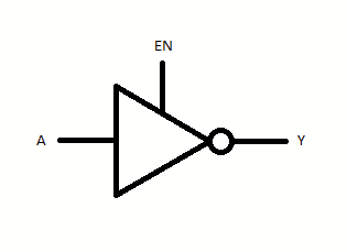
In order to implement a high impedance node on a bus, you need a logic-controlled switch that can fully disconnect your peripheral from the network.
Unfortunately, you don't seem to have that here. Every symbol on the page drives the bus either to your high logic voltage level, or to low.
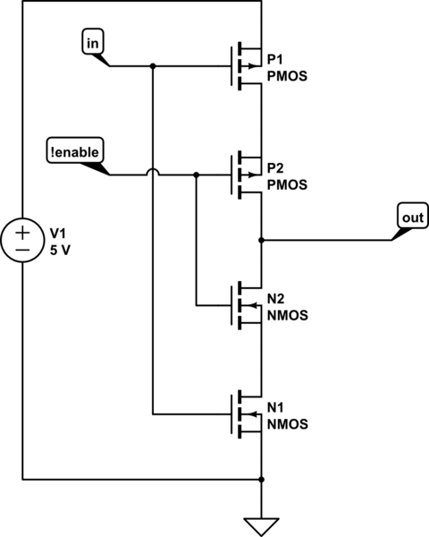
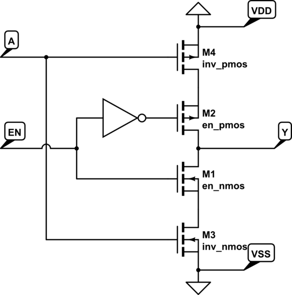
In a real circuit, you can implement this kind of switch with a pair of MOSFETs and another inverter like this example of a tri-state inverting buffer:

simulate this circuit – Schematic created using CircuitLab
The input signal, \$A\$, controls the two outermost MOSFETs. When \$A\$ is high, its connected nMOS conducts; when low, the pMOS conducts. The \$EN\$ signal turns on its connected nMOS when high, and is inverted to turn on its connected pMOS when low. I've drawn the inverter as an inverter here for clarity, but it's really just two more complementary MOSFETs, to make a total of six.
Often, this is simplified as a logic symbol which has a buffer with a third input coming out of the bottom, like so:

Since a symbol like this doesn't appear in your list, you can't really implement tri-state logic.
