0
\$\begingroup\$

I'm working on my home project of building the 8-bit computer and now I'm on the RAM building stage. I'm going to use this chip for as my RAM UTRON UT62256C (datasheet). This chip is to be connected to the common bus, to which 8-bit registers are connected through 3-state buffers. My question is about write cycle timings (see the diagram below) enter image description here
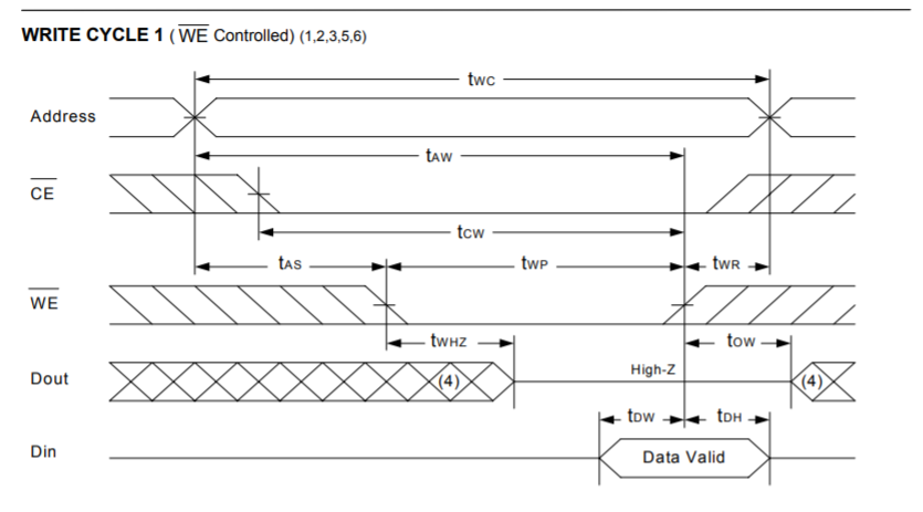
The doc says that after !WE goes down there is a period of time twhz when signals on I/O pins must be not applied: "4.During this period, I/O pins are in the output state, and input signals must not be applied. "

Question #1: Does that mean that I CAN NOT set-up the data upfront and then just put the !WE low for some period of time? If I do so, will it damage the chip?

Having said that !CE is to be always LOW, I assumed that my write cycle could look like this:

  • Set up the address using
  • Set up the data on the bus
  • Make !WE low for certain period of time.

As it's an educational project I wanted write cycle to be like this because it simplifies design for manual mode of putting data to the SRAM. I was going to use dip switchers to set up the data and the address and one button to move !WE from High to Low maybe with 555 timer to set-up the pulse length.

Question #2: If I must not put the data on I/O pins before twhz, I was thinking about could you please advice some circuit that will allow to do manual programming with dip switchers

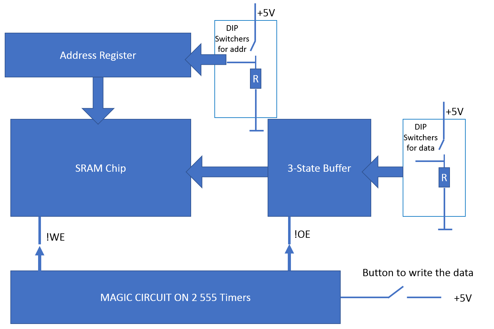
I was thinking about adding 3-state buffer between I/O pins and the dip switchers and some circuit that generates two pulses with the right timings triggered by pushing the button:

  • First !WE goes down for certain period of time for example 555 timer could be used.
  • !WE pulse triggers the second 555 timer that generates !OE pulse on the 3 state buffer.

See the picture below. Looks like overcomplicated thing :) enter image description here
Thanks for you replies in advance.

\$\endgroup\$
2
  • \$\begingroup\$ I suggest you put up the timing of the read-cycle. Have a careful look at that and specific check on what signal edge(es) the data out goes tri-state and how long it takes (the maximum data-out hold time ). From that you should be able to figure out when it is safe to put your data on the bus. \$\endgroup\$
    – Oldfart
    Commented Jul 23, 2019 at 15:06
  • \$\begingroup\$ Thanks for you reply. The chip has the same pins for input and output. \$\endgroup\$ Commented Jul 23, 2019 at 15:26

3 Answers 3

3
\$\begingroup\$

The doc says that after !WE goes down there is a period of time twhz when signals on I/O pins must be not applied: "4.During this period, I/O pins are in the output state, and input signals must not be applied. "

This is a poorly written data sheet. While the concern mentioned can exist, the previous note #3 does a poor job of expressing the reality that the problem only exists if the /OE is held low throughout a write, which would not be a common or generally wise practice.

Typically, in a processor bus of this era, the chip select /CS would be driven active low by an address decoder subject to contamination and glitching during the change of the address lines from one value to another. As a result, a /CS timed write is not generally used. Nor is it a good idea to have a memory chip driving the data bus surrounding a write cycle, so /OE would not be tied low and the quoted concern would not exist.

Instead, the typical approach is to have the bus master drive the /OE line only if it wished to perform a read operation, and to drive a properly timed strobing of the /WR line at the proper time in a write cycle.

By using /OE to control the output buffers, and using /WR to the time the writes, you should be able to avoid conflict and be able to safely drive the data lines during all periods of time except those surrounding assertion of the active low /OE signal. Of course, to read from the memory, you will need a way to disable whatever you use to drive the data lines during a write, and to make sure that those drivers are disabled for a safe window around the assertion of /OE.

You are always able to drive the address lines, but their values only matter at the times required before/during/after a write or read cycle.

A simple way to construct a deterministic memory interface may be to create a finite state machine and include the clock low period as a factor in the generation of /OE, its complement to the write data drivers, and /WR. Keep in mind that a processor itself tends to be a sort of state (or else microprogrammed) machine - with instructions needing multiple clocks (or at least clock phases) to complete. You really only get to one instruction per clock with heavy pipelining and when operating from distinct internal code and data caches.

\$\endgroup\$
2
  • \$\begingroup\$ Thanks a lot for so comprehensive answer. Just to double check that I got the whole thing correctly, if we imagine that !OE stays high for relatively long time already, I can set any data on I/O pins as they are suposed to be in High-Z state. Once the address and the data are ready I can have a pulse of certain length on the !WE pin and write cycle will be completed and it's safe for the SRAP chip itself. \$\endgroup\$ Commented Jul 23, 2019 at 20:03
  • \$\begingroup\$ Yes, you only risk a conflict if something else is driving the data lines during or in the vicinity of a time when /OE is low. \$\endgroup\$ Commented Jul 23, 2019 at 21:11
1
\$\begingroup\$

The other kind of write cycle ("Write Cycle 2", controlled by CS-) might be a better fit for your overall system design.

With the chip deselected (CS- high), you apply the address, data and WE- low all at the same time. Then you pulse CS- low and then high again while holding those other signals steady.

\$\endgroup\$
1
  • \$\begingroup\$ If this is going to be done, then /CS cannot simply be driven by an address decoder as it will glitch during transitions - something with proper strobe timing would have to be included. In typical processor busses of the era, that would be a /WR strobe. \$\endgroup\$ Commented Jul 23, 2019 at 15:20
0
\$\begingroup\$

To put it simple: The typical setup is

in case your µC has distinct –RD and –WR outputs (e.g. Z80)

  • wire the address decoder output to the –CS input of the RAM chip.
  • wire the –WR output of the µC to the –WE input of the RAM chip.
  • wire the –RD output of the µC to the –OE input of the RAM chip.

in case your µC has an R/-W output (e.g. 6502)

  • wire the address decoder output to the –CS input of the RAM chip.
  • wire the R/-W output of the µC to the –WE input of the RAM chip.
  • wire the inverted R/–W output of the µC and the –CS input on the RAM chip though an OR gate to the –OE input of the RAM chip.

No further magic needed. If you happen to need any delays for more exotic chips —none come to my mind prominently—, you don't do that with an NE555 or similar but with the propagation delay of inverters, which is in the 5ns range for the 74xx gate series and in the 40ns range for the 40xx gate series at 5V.

\$\endgroup\$
3
  • \$\begingroup\$ Thanks for your reply. Actually I'm not using any microcontroller, I'm kind of building my own for educational purposes. So far I have a common bus, a couple of registers, ALU and now I'm trying to hook up a SRAM. Thing that makes it a little bit more complex is that I want to be able to program the SRAM manually through DIP switches. \$\endgroup\$ Commented Jul 23, 2019 at 20:08
  • \$\begingroup\$ Like set address on the switches, set data on the switches, push some button and get the data stored in SRAM. So in this way I can manually enter the commands into the SRAM and then execute it either running clock in automated mode or through pushing button, so that I can see what exactly changes. For that purposes I have bunch of LEDs almost everywhere :) \$\endgroup\$ Commented Jul 23, 2019 at 20:09
  • 1
    \$\begingroup\$ In that case, just lock –WE and –OE against each other. Your dip switches must be disconnected from the data bus when –OE is active. You can do this with one 74244. \$\endgroup\$
    – Janka
    Commented Jul 23, 2019 at 20:50

Your Answer

By clicking “Post Your Answer”, you agree to our terms of service and acknowledge you have read our privacy policy.

Not the answer you're looking for? Browse other questions tagged or ask your own question.