0
\$\begingroup\$

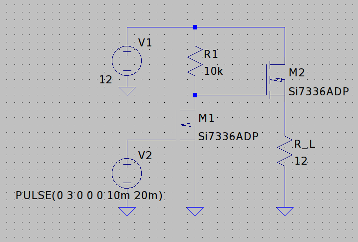
I'd like to dim an ordinary 3-pin PC fan with a 3.3V-PWM at its 12V power supply pin. As I also need to measure the tachometer signal within a 3.3V logic level circuitry I'd like to switch the fan on the high side. Otherwise the tachometer signal will be pulled to 12V which is what I'd like to avoid. Untill now I don't have any PMOS on my BOM, but I already use several NMOS. That's why I came up with the following circuit which seems to work as intended corresponding to my LTspice simulation. But I'm unsure if there might be any hidden disadvantages or complications that are not revealed by my simulation.

Is such a circuit ok?

enter image description here

The MOSET I'm going to use is the CSD17382 of TI.

\$\endgroup\$
3
  • \$\begingroup\$ You're exceeding the Absolute Maximum Ratings with respect to \$V_{GS}\$ for M2. You can solve it by using a voltage divider. \$\endgroup\$
    – Huisman
    Commented Aug 12, 2019 at 20:14
  • \$\begingroup\$ @Huisman oh, you're right! Thanks for the hint and your solution! But in general there are no disadvantages compared to the common P-MOS circuit (despite the fact that I need one more MOSFET)? \$\endgroup\$
    – Sim Son
    Commented Aug 12, 2019 at 20:17
  • 1
    \$\begingroup\$ Regarding the simulation in LTspice: You can download the pspice model for the CSD17382 from the website of TI. \$\endgroup\$
    – Huisman
    Commented Aug 12, 2019 at 20:43

4 Answers 4

1
\$\begingroup\$

None of the PWM chop approaches really work, be it high-side or low-side. Why? Because the chop disrupts the motor control IC and messes up the tach signal.

What this means is, you need a different approach to controlling the fan speed than duty cycle: you can regulate its current or its voltage.

I faced this issue a while back on a RAID enclosure with a fan. Here's what I did:

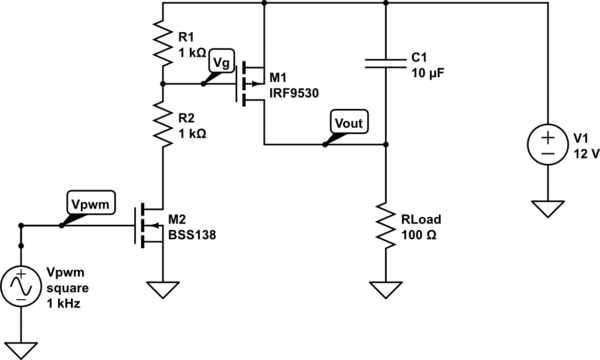
schematic

simulate this circuit – Schematic created using CircuitLab

What this circuit does is provide a gross series resistance control to the fan. Between PWM cycles, Vout will decay to some value, but not so low that the BLDC IC conks out. Tune C1 to achieve this minimum value for the lowest duty cycle you want to support (say, 25%.)

It looks weird, but it works well and has the benefit of not kicking PWM noise back onto the +12V line as the C1 discharge loop is local to M1.

I don't think it will work with an N-FET and bootstrapped drive as the bootstrap will decay when the PWM is at 100%.

That all said... is a 4-wire fan completely out of the question?

\$\endgroup\$
4
  • \$\begingroup\$ Thanks for sharing your experience! My final circuit is actually similar to your's, except that I don't have C1 till now (which is the essential difference, I know ;). Are you sure the noise on the 12V-line isn't caused by missing a freewheeling diode, which I guess is mandatory (or is it usually included in the fan's internal circuitry anyway?)? \$\endgroup\$
    – Sim Son
    Commented Aug 13, 2019 at 0:35
  • \$\begingroup\$ "is a 4-wire fan completely out of the question?" - the idea is to provide both 3- & 4-pin fan rpm control... \$\endgroup\$
    – Sim Son
    Commented Aug 13, 2019 at 0:41
  • \$\begingroup\$ BLDC motors don't need freewheeling diodes, they have them built in to the coil drives. You only need the diode for a brush motor. As for the noise, flyback was the first place I looked. It doesn't happen with BLDC. Instead, the BLDC motor itself has turn-on inrush - caps to charge, etc. This kicked back on the line when the FET turned on, not when it turned off. \$\endgroup\$ Commented Aug 13, 2019 at 1:58
  • \$\begingroup\$ That's interesting! Luckily, I mentioned that I'm interested in the tachometer signal, otherwise I would probably have taken an unsuitable solution! \$\endgroup\$
    – Sim Son
    Commented Aug 13, 2019 at 4:35
3
\$\begingroup\$

In this configuration, the maximum voltage you can get across the load resistance will be equal around: \$12V - Vgs = 10.5V\$. Also, the power losses in the MOSFET will be higher than normal.

\$P_{tot} = V_{GS}*I_D \approx 1.5W\$ instead \$P_{tot} = Id^2*R_{DS(ON)} \approx 65mW\$

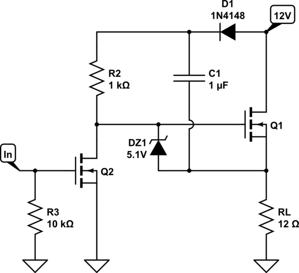
I recommend adding a MOSFET bootstrap circuit and a Zener diode to limit the \$V_{GS_{max}}\$ (below 10V)

schematic

simulate this circuit – Schematic created using CircuitLab

\$\endgroup\$
3
  • 2
    \$\begingroup\$ Unless there is a limitation that prevents switching on the low side as opposed to the high side, a simpler solution would be to move Q1 down, swapping its position with the load. This way, the N-FET would have its source connected to GND, as they like to have :). \$\endgroup\$
    – joribama
    Commented Aug 12, 2019 at 21:21
  • \$\begingroup\$ Thanks for your suggestion! I guess the bootstrap circuit will require a continuous switching, so what about 0%/100% duty cycle? Unfortunately this circuit will as well introduce some new components to my BOM and I would then prefer using a P-MOS high side switch. Thanks for your solution anyway!! \$\endgroup\$
    – Sim Son
    Commented Aug 12, 2019 at 22:03
  • \$\begingroup\$ This will not work correctly when the duty cycle is 100%. C1 will discharge though leakage via itself, DZ1, and even Q2, until Q1's gate voltage reaches 12V-0.6 = 11.4V. Not what you want. \$\endgroup\$ Commented Aug 13, 2019 at 4:34
2
\$\begingroup\$

You're exceeding the Absolute Maximum Ratings with respect to \$V_{GS}\$ for M2. You can solve it by using a voltage divider.

Typically, a disadvantage of using a NMOS as high side switch is that because the voltage at the source (almost) equals the voltage at the drain when it is conducting, you need a gate voltage that is higher than voltage at the drain to get a decent \$V_{GS}\$.
When applying the maximum 10V on the gate (or even 12V if it wouldn't violate the Abs Max ratings), you will not achieve this. You need a charge pump or equivalent circuit to decently drive M2.
A disadvantage of such a charge pump is you cannot use it on 100% PWM: there is an off time required to recharge the charge pump's capacitor.

\$\endgroup\$
1
\$\begingroup\$

This is not a very good solution because of the power dissipated on M2.

Let me elaborate... To turn M2 on, you need Vgs>Vth. The FET you chose (CSD17382) has a very low Vth, 0.9V, what is a good thing. It's fair to assume that Vg=12V (when M1 is off) since the gate current is negligible. So, in order for M2 to have Vgs=0.9V, it needs to develop a 0.9V drop across Vds. So if Vd=12V, Vs will end up being 11.1V so that the FET actually starts conducting current. The power dissipated on the FET will then be Vds x Iload. Assuming a load of 1A, we are talking about 0.9V x 1A = 0.9W, which is more than what the FET can handle.

My recommendation is that you swap the position of the load and M2, so that M2's source is connected directly to ground. This way, the FET will be fully saturated when M1 is off, reducing the dissipated power to (Iload^2)*RDSon, in the order of 50mW in your case. You should also add a resistor between M2's gate and GND to form a voltage divider with R1, so that you don't exceed Vgsmax=10V, as @Huisman already pointed out. I would aim at Vgs=8V.

\$\endgroup\$
3
  • \$\begingroup\$ Thanks for your explanation! I don't know if I got you right: if I "swap the position of the load and M2" my circuit will be a low-side switch again which is what I explicitly don't want. I could then also implement an ordinary N-MOS low-side switch using only one MOSFET... \$\endgroup\$
    – Sim Son
    Commented Aug 12, 2019 at 21:56
  • \$\begingroup\$ ... the thing is: in an off-state, the entire fan (including the tachometer signal) will be on a 12V-level \$\endgroup\$
    – Sim Son
    Commented Aug 12, 2019 at 21:59
  • \$\begingroup\$ You are correct. My proposal is to use a low-side switch instead, and as you said, you could even use just one FET in that case. I'll take your word when you say you can't use a low-side switch. If you really need high-side switch you're limited to two options: simply use a single P-FET instead (the RDSon will be slightly higher than an N-FET for a given size, but it should not be a big deal for you); or use an N-FET with a gate driver boost as illustrated in @G36 's reply. \$\endgroup\$
    – joribama
    Commented Aug 12, 2019 at 22:25

Your Answer

By clicking “Post Your Answer”, you agree to our terms of service and acknowledge you have read our privacy policy.

Not the answer you're looking for? Browse other questions tagged or ask your own question.