1
\$\begingroup\$

I'm working on a project to control power sideview mirrors in a car, with features like TildDown, that tilts some of the mirror down helping to park. The circuit is pretty simple, but I'm having some difficulty to turn the power mirror motors with my microcontroller.

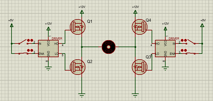
It needs to be a Half H-Bridge kind of circuit for powering the motors because each motor pin needs three states: VCC (+12V), GND and high impedance (opened). In that case, I'm having two outputs of the microcontroller for each motor pin, one to toggle between the High and the Low Mosfet and the other to act as an enable for the Half H-Bridge, so when it is in '0' none of the Mosfets gets triggered and the Motor won't turn on doesn't metter the voltage of its other pin.

Half H-Bridge Driver Application Schematic

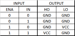
So I need a driver, that accepts a 5V input and an around 12V output, to connect my microcontroller to the Half H-Bridge, with the following truth table:

![Driver Truth Table

I have seen some Half H-bridge Driver ICs, like the IR2104, but it seems like they are indicated for PWM application, which isn't the case. I'd like to know if there is a driver similar to the one I'm looking for or if there is any other solution for the problem. I know it may seem confusing why it can't be a simple mosfet activating the motor with VCC and GND, it is because the motor of the power mirror have a common wire and I need to control each one individually, so I need the phase pin of the motor that I don't want to move to be high impedance while the phase pin of the other motor is in GND for example (which is exactly what the power mirrors switch does in the car circuit for controlling each mirror individually).

Thanks in advance and sorry for the bad english!

UPDATE

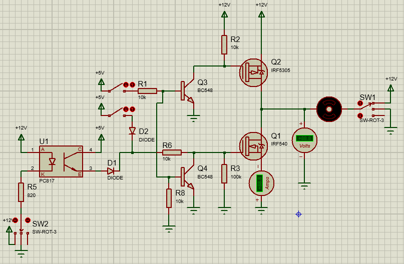
Due to all the tips received, I think I finally have a working circuit. As you can see in the schematic picture, the output has the three stages: VCC, when the input thats connected to Q3 (which will be an output from the microcontroller) is in +5V; GND, when the input connected to Q1's gate (also an output from the microontroller) gets high or when optocoupler out put gets high (controlled directly by the power mirror switch, allowing the mirror pin to be GND in manual adjustments); and the most important, if none of these signals get high the motor pin floats and it won't conduct. I've also added the bipolar Q4, that completely turn off the Mosfet Q1 when the high side signal is on, doesn't metter the value of the other signals, avoiding both Mosfets being activated at the same time, causing a short circuit in the +12V supply.

Three Stages Mosfet Driver

I've tested the circuit in a protoboard and it worked perfectly, it also drains almost any current from the digital signals (around 10mA, which is good for Atmega328p outputs). I'm planning to use smd components in the final project (SOT23 package): for the bipolar I'm using BC817, and for the mosfets I'm using SI2319DDS and PMV55ENEAR, channel p and n respectively. I looked at the Mosfet's datasheets and they seem to be appropriate due to its low RDSon and high ID current. I'm just concern about the evetual eletromagnetic noise in the car that can trigger the Mosfets unwanted because of the low VGS threshold.

If someone know some issue I may have because of the circuit desing or because of this components in the automotive enviroment, please, let me know. Thanks for all the help!

\$\endgroup\$
2
  • \$\begingroup\$ Typically any driver designed to drive 2 N FETs requires PWM, because internal circuitry requires the low side FET be on occasionally in order to charge up what's called a bootstrap circuit to drive the high side. if you just want to be able to leave the high side on continuously, consider a design that uses a P FET. \$\endgroup\$
    – MadHatter
    Commented Sep 7, 2019 at 16:03
  • \$\begingroup\$ somewhat related: Bootstrap gate drivers \$\endgroup\$ Commented Sep 8, 2019 at 18:42

2 Answers 2

1
\$\begingroup\$

Your circuit won't work because you have failed to account for the fact that MOSFETs are controlled by the voltage DIFFERENCE between their gate and source pins. The voltage you are applying to the gate is relative to ground, so if the source pin is also connected to ground then you have no problems since the voltage you are trying to apply to the gate is relative to ground, and the voltage the MOSFET cares about (the gate-source voltage) has been forced to be relative to ground (like with Q2 and Q3).

But this is not the case with Q1 and Q4. Suppose Q1 or Q4 did actually turn on properly and current flows through the load. A voltage drop develops across the load with one end of the load being connected to ground (via Q2 or Q3). So what happens to the voltage of the source pin of Q1 or Q4 relative to ground? How does this affect the difference of the voltage between the gate-source? And what happens if you are applying a gate voltage that is relative to ground, but the source pin voltage relative to ground is no longer at ground?

Try and think about it carefully and see if you understand why Q1 or Q4 can never actually turn on completely or properly. If you are stuck, see here: Why choose a PMOS over an NMOS or vice versa?

Think something like a source follower.

Or think about an electromechanical relay. It has two coil pins for control and two contact pins for the primary power flow. You would never ever apply a signal to one of the coil pins while ignoring the other coil pin and expect it to work right?

A transistor is the same, except one of the coil pins and one of the primary contact pins is fused together (the source pin on a MOSFET is a bit like a fused version of a relay coil pin and contact pin). That means you cannot apply a voltage to the gate and expect it to work without taking into account the relationship with the source pin. That's pretty much what you are doing here.

Unlike a relay, since a control and primary current flow pin are fused in a transistor, it means that any load connected to the source pin can influence the requirements of the control signal so your gate drive requirements can get trickier.

So you either need a gate-drive that supports a bootstrap capacitor and and diode use it with a bootstrap capacitor, or substitute the bootstrap capacitor/diode with an isolated regulator that floats (more expensive but is required to allow 100% duty cycle since bootstrap capacitors require the Q1 and Q4 to periodically turn off and Q2 and Q3 to periodically turn on in order to refresh the charge on the boostrap capacitor (this provides a connection that connects the bootstrap capacitor between GND and the power supply to recharge it). This last paragraph probably won't make too much sense to you until you go and find a high-side gate driver IC and look at the schematic for. So go do that.

\$\endgroup\$
3
  • \$\begingroup\$ I think I got it! Thanks to your explanation I realised that a P channel Mosfet (for Q1 and Q4) is much more appropriate for the usage in this case. Dispite that, it would still be good to have some sort of driver to, first of all, put around 12V on both Mosfets gates with only 5V logic inputs and also to avoid activating both of the Mosfets at the same time (if you apply GND and VCC in the P channel and N channel gates respectively) what would cause a short in the 12V supply. \$\endgroup\$
    – Roga
    Commented Sep 7, 2019 at 17:25
  • \$\begingroup\$ @Roga Well, a PMOS does make it a bit easier. The NMOS is more efficient though and they are more available. If you use a PMOS in this way, pay attention to the maximum gate-source voltage. it has to be at least as high as your Vmotor if you are planning on pulling the gate all the way down to ground to turn it on (which is the simplest). If Vgsmax is not high enough then you need extra circuitry and you might as well go NMOS with a high-side drive at that point. You want a gate driver regardless if you plan on PWMing so the transistors can turn on and off fast enough. \$\endgroup\$
    – DKNguyen
    Commented Sep 7, 2019 at 18:04
  • \$\begingroup\$ There are a very few drivers out there that will do high-side drive of an NFET in always-on mode. They either have a charge pump built in, or you have to supply them with a higher voltage from your own boost converter (which doesn't need to supply a lot of current). I think I'd do this job with PFETs on the high side, though. \$\endgroup\$
    – TimWescott
    Commented Sep 7, 2019 at 18:04
0
\$\begingroup\$

Answer to the update:

You should be fine about EMI triggering the gate. You can always decrease the gate pull resistors to 10K or even 5K. Or add a a small capacitor between the gate-source to artificially increase the gate capacitance so it takes more EMI to trigger the gate. This works because slower switching speed is not a concern here since you aren't PWMing at high frequency so switching happens infrequently so extra heat from slow switching is minor.

\$\endgroup\$

Your Answer

By clicking “Post Your Answer”, you agree to our terms of service and acknowledge you have read our privacy policy.

Not the answer you're looking for? Browse other questions tagged or ask your own question.