15
\$\begingroup\$

What methods might be feasible for attaching/stacking one PCB immediately on top of another PCB, with the following conditions:

  • Zero spacing/gap between the two PCBs
  • Electrical contacts are needed, not just physical attachment
  • Assume that the top PCB is about a third the size of the bottom PCB

I'm at the early design stage of a project and am trying to survey the options first, so I'm open to recommendations of standard methods as well as any creative ideas.

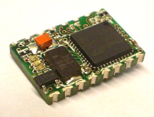
Note: I'm already familiar with edge castellations (AKA "half vias"), so other suggestions would be of interest.

For instance, is it possible to design it such that the top PCB has pad-contacts only at the bottom (QFN/QFP style) which are somehow solderable onto pads on the bottom PCB?

EDIT: To answer @Andrew's question:

My purpose of stacking the two boards like this is that the Top PCB will be variable across variants of my device (in fact, variable not only in what the Top PCB contains but also size and number of contacts it has), hence the goal of having one constant Base PCB with pads onto which I can attach a variable Top PCB.

\$\endgroup\$
3
  • \$\begingroup\$ I have to ask: Why? assuming you must have the space on the main board to fit the daughtercard... whilst this may be technically possible, I'm concerned from a manufacturing/assembly viewpoint, especially with your "somehow solder" comment. \$\endgroup\$
    – Andrew
    Commented Oct 29, 2012 at 10:37
  • 1
    \$\begingroup\$ @Andrew: Added answer to your question above. And what is the concern from the assembly viewpoint? Very likely this is not an uncommon setup (?) \$\endgroup\$
    – OrCa
    Commented Oct 29, 2012 at 10:56
  • 4
    \$\begingroup\$ I'd say this is a very uncommon approach, usually people use connectors or castellation as you say. You could do what you are talking about like a QFN. A real QFN is essentially just a tiny pcb with a die on top and pads on the bottom. One major difficulty with something this size will be coplanarity. Your boards will have to be very flat in order to be assembled easily, and I assure you they are not flat enough by default ;) IPC class 2 allows for some bow/twist of the board, and during reflow they will flex and twist as well. The bigger they are the harder this will be to assemble. \$\endgroup\$ Commented Oct 29, 2012 at 14:39

5 Answers 5

15
\$\begingroup\$

This is not a direct answer to your question, but I think it's quite relevant.

A few years ago, we did the same thing. We made little daughter boards that used edge castellations to solder it onto the mother board.

EtherCAT SPI Module

The difficulty was that we had components on the bottom side of the PCB. These were the vital decoupling capacitors needed by the chip.

So the motherboard had very large vias to accommodate these components.

EtherCAT Motherboard

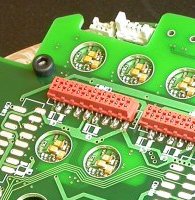
You can see several large round holes in the PCB. Through the holes you can see the capacitors on the flip side of the daughter boards. Since the holes are just large vias, they end up through-plated (our supplier doesn't offer unplated holes), so you have to be careful that the plating doesn't short any pads on the daughter board.


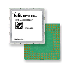
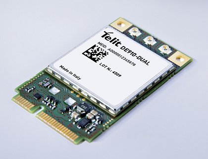
A few thoughts about using pads under the PCB. I assume you mean something like this Telit HE910 module:

Telit HE910 Telit HE910 Soldered

Which reflow solders directly onto a PCB. Notice that in the picture the gap between the module and main PCB is not zero, but certainly less than 1mm. Clearly this technique works. Whatever components are inside the module don't mind undergoing an extra reflow process. This is because components can usually survive at least two reflows (once for each side of the board). Since those modules only have components on one side of the PCB, they have almost certainly experienced only one reflow.

Instead of reflow, you might be tempted to use a hot plate to solder a module like this. This would enable you to solder the module down without getting the components inside the module too hot. However, I would advise against this method. At the moment the solder solidifies, the mother PCB will be much hotter than the daughter PCB. As the mother cools and shrinks, it will generate shear forces in the solder joints, and may warp.

\$\endgroup\$
8
  • 1
    \$\begingroup\$ One potential solution to this is that he could solder the raw PCBs together first, then populate and reflow the boards. It doesn't add much in the way of quick mix-and-matching but it would help against having to require components to endure a second reflow cycle. \$\endgroup\$ Commented Oct 29, 2012 at 14:10
  • 7
    \$\begingroup\$ I like that you drilled giant holes in the mother board to accommodate the decoupling caps, that's pretty awesome. \$\endgroup\$ Commented Oct 29, 2012 at 14:23
  • 1
    \$\begingroup\$ Well, we made castellations the bad way (use vias on the outline of the board). The problem is that, when the board is routed, it tears the plating from the vias. They were very unreliable. A nightmare. It's best to get your PCB manufacturer to make them properly for you. If you can't do that, then expand the board outline so that the vias are left intact, then use a belt sander to sand away half the vias. This reduces stress on them. \$\endgroup\$ Commented Oct 29, 2012 at 21:52
  • 1
    \$\begingroup\$ They're probably still vulnerable to things like thermal and mechanical stress. You might consider: 1) strengthening the copper around the castellation with a couple of small vias. This helps to rivet the copper down. 2) have all castellations along one edge, and use some flexible glue along the other edge. This should relieve some mechanical stress on the solder joints. However, I should say that I have no long term experience with proper castellations in any kind of rugged environment. Maybe someone else has? \$\endgroup\$ Commented Oct 29, 2012 at 21:57
  • 2
    \$\begingroup\$ @Sener - These are IDC wire-to-board connecrtors called Micro-Match by TE-Connectivity. \$\endgroup\$ Commented Nov 7, 2018 at 11:08
5
\$\begingroup\$

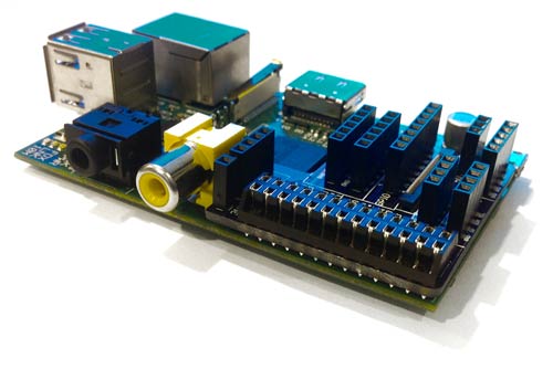
Maybe not exactly what you are asking, but I suggest you to check out PiCrust for ideas. They use connectors by Hirose to achieve a compact stacked design on top of the Raspberry Pi board.

If the board should be replaceable without soldering, this sounds like a pretty simple solution to the problem.

Picture of PiCrust Board

\$\endgroup\$
3
\$\begingroup\$

In my (admittedly narrow experience) daughter cards are usually fitted on header connectors, not directly soldered.

In reply to a question about Very low stacking height PCB connector, @trygvis suggested this Molex connector

Maybe that's of use?

The problem with face-to-face soldering as you describe is that this will have to be a manual process (not pick-and-place with reflow) unless you want to reflow your PCBs. Also, you would need to be sure of the mechanical fixing - a few solder tags probably won't be enough - you will need mechanical fixing otherwise there is a serious risk of vibrarion fracture.

\$\endgroup\$
1
\$\begingroup\$

Two principal things come to mind:

1) what is you describe could be used to allow describe a solder bump (BGA) type package that uses a FR-4 substrate. This is not an uncommon packaging option.

2) there used to be a type of tape that you could get that would preferentially enhance electrical connection through the thickness of the tape whilst minimizing lateral conduction. I used to be available from 3M, but I haven't seen it in years. And it's conductivity was probably insufficient for your use if you need to carry 100's of mA. This might give you an idea or two.

\$\endgroup\$
1
  • \$\begingroup\$ Re #2: You're thinking of 3M Z-Axis tape. It only conducts vertically between boards, not horizontally between pads. \$\endgroup\$
    – Navin
    Commented May 17, 2019 at 6:03
1
\$\begingroup\$

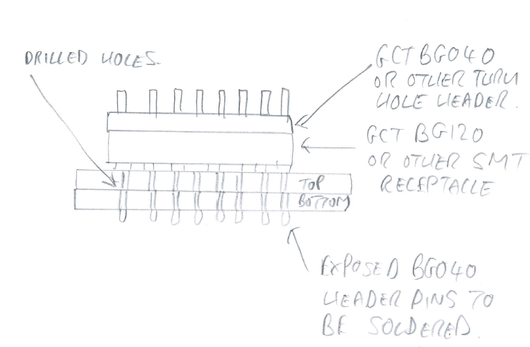
You might consider using a combination of SMT receptacle and thru hole pin header, for example:
2.54mm DIL SMT socket BG120
2.54mm DIL Thru hole pin header BG040

You could choose single row, GCT also offer finer pitches if required, other options here.

-Mount the SMT socket on the top PCB.

-Plug a thru hole pin header (from above) all the way through both PCBs. Obviously the mating pin header pins should be long enough to pass through the SMT female receptacle, both PCB's and leave you enough space to hand solder.

-Hand solder the exposed header pins on the bottom side of the bottom PCB.

See sketch enclosed (excuse my awful drawing)enter image description here , I'm not sure if this will work for you, just an idea!

Note: GCT standard products available via Newark, any non standard pin lengths carry a higher MOQ (at least 1k pieces).

\$\endgroup\$

Your Answer

By clicking “Post Your Answer”, you agree to our terms of service and acknowledge you have read our privacy policy.

Not the answer you're looking for? Browse other questions tagged or ask your own question.