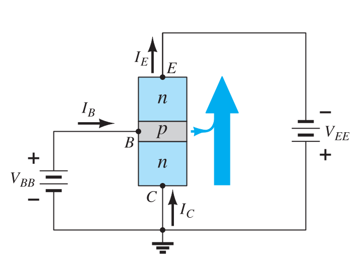
This is the circuit diagram of an n-p-n BJT in Common Collector configuration, taken from the book :-

I know that for the transistor to operate in active mode :-
the Emitter-Base junction should be forward biased.
the Collector-Base junction should be reverse biased.
By looking at the diagram, I can see that the Emitter-Base junction is forward biased. But I am unable to understand how the Collector-Base junction is reverse biased, since the Base is connected to the +ve terminal of VBB and the collector is at zero potential ( looks like forward biased to me ) .


