1
\$\begingroup\$

I'm creating some circuits required in a student-built electric-vehicle application. There are no heavy loads on the low-voltage +12V system.

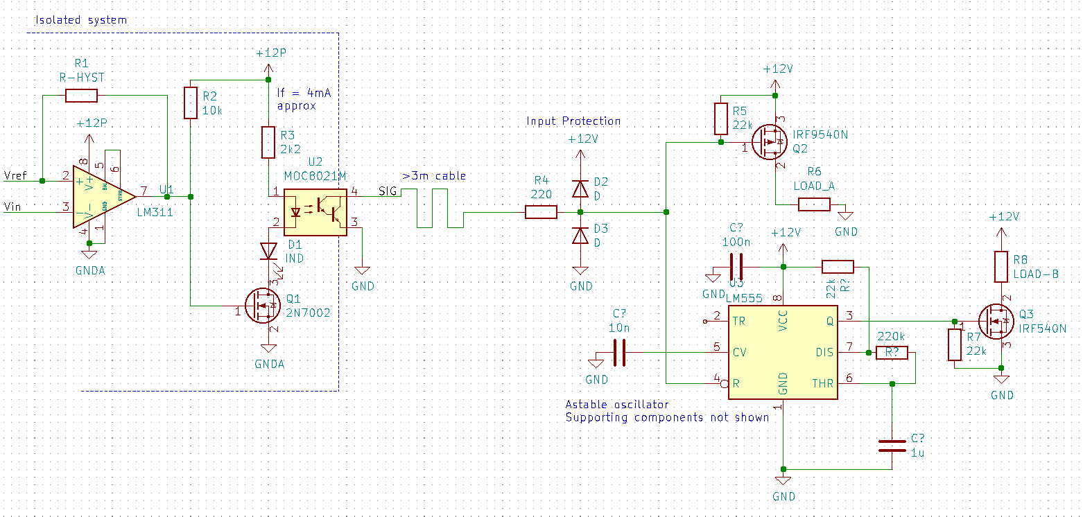
What I have below is a circuit that does some threshold detection (LEFT), which indicates that status to an isolated output-circuit (RIGHT).

schematic diagram

The intention here is that U3 (LM555) and Q2 (IRF9540N) should act in a complementary way to each other:

  • SIG=LOW => Q2 ON

  • SIG=HIGH => U3 ACTIVE

I've tested this output circuit using a relay to switch SIG to ground, and that works well!

In attempting to iterate a solid-state-only design, I attempted to replace the relay with darlington optocoupler U2 which produces the following effects:

  • When SIG is pulled HIGH (R5), U3 is active and Q2 is OFF - as expected.

  • When comparator U1 triggers, driving optocoupler U2 @ ~4mA, SIG is not pulled entirely to ground - rather, about 0.5V as measured with a multimeter. This appears to be enough to (partially) activate both U3 and Q2. Q2 is clearly on because Vgs is much less than Vgs(th). What's curious is that U3 appears to drive LOAD-B on.

    Does this imply that there is some oscillation in SIG or at least at the ENABLE pin of U3? I would have expected the chip to be either active (oscillating) or not. Not some intermediate state.

I have a few ideas on how to improve this circuit, but was wondering what readers here might think.

Specifically, my questions are:

  • Is this a naive approach to creating a voltage-robust input in the right-hand circuit? I want to protect somewhat against noise and wiring mishaps.
  • Is the 0.5V an artefact of some minimum Vce that is possible across the optocoupler? Remember, substituting a relay or switch works perfectly. I'm a lot more comfortable working with MOSFETs than BJTs (and therefore optos) - this is honestly my first time trying to use one.
  • Is a viable solution to schmitt-trigger on the right-hand side's input to create a purely digital signal, and therefore create a strictly complementary operation of Q2 and U3?

Note: supporting components for U3 555 timer now shown to avoid ambiguity.

\$\endgroup\$
3
  • \$\begingroup\$ To clarify, the optocoupler must remain in the left-hand circuit. There is a requirement for the signal to be isolated there. \$\endgroup\$
    – Michael
    Commented Oct 5, 2019 at 11:35
  • \$\begingroup\$ We discourage broad, open-ended design review questions here on EE.SE, because the answer(s) tend to become long strings of unrelated edits and/or comments. While this might help you with your immediate problems, it is of no value to the site overall. We DO allow design review questions in which you explain your choices and then focus on a few points about which you still have doubts. To get a better feel of what is or is not acceptable, search for "design review" on the meta site. \$\endgroup\$
    – Dave Tweed
    Commented Oct 5, 2019 at 11:39
  • \$\begingroup\$ @DaveTweed I'll review the meta and modify my post to suit. \$\endgroup\$
    – Michael
    Commented Oct 5, 2019 at 11:51

2 Answers 2

1
\$\begingroup\$

EDIT: The changes to the question completely addressed my earlier points. Now we can talk about the new details.


A Darlington pair by definition cannot have the low saturation voltage of a single BJT, or the equivalent low on-resistance of a MOSFET. You can get optoisolators with MOSFET outputs, which might suit your application better.

The reset input of a 555 is not a TTL-compatible pin. This becomes obvious if you look at the schematic in the datasheet. Unfortunately, I've never seen an actual specification of what VIL(max) or VIH(min) are for this pin — the datahseets seem to assume that you're tying the pin directly to either Vcc or Gnd. Again, a MOSFET-based isolator would probably help here.

\$\endgroup\$
2
  • \$\begingroup\$ Good catch on Q2 orientation. I redrew for this post and missed that. I'll include the missing parts too to make that clear. The ~RESET pin is being used as an enable/disable only. So not strictly the same as the design tool. \$\endgroup\$
    – Michael
    Commented Oct 5, 2019 at 11:44
  • \$\begingroup\$ Thanks for your input, Dave. I agree that a MOSFET optoisolator would be more appropriate, giving a "true" open-drain output. I've implemented a bodge for now, with a view to both re-spec the opto and think harder about the input circuit. If you're curious, you can see my bodge in my answer. \$\endgroup\$
    – Michael
    Commented Oct 6, 2019 at 11:45
1
\$\begingroup\$

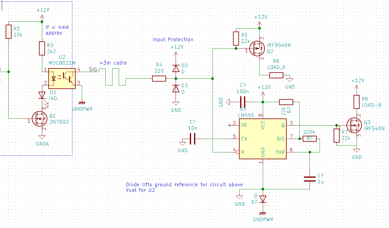
A bodge solution that I am proceeding with for now is as follows: Raise the ground node of the timer circuit using a diode on the negative supply connection. Now the Vsat for the darlington output of U2 corresponds to an acceptable VIL at the ENABLE pin of 555 U3.

enter image description here

This is a temporary solution, giving the desired behaviour for now. Clearly, both the output and input circuits should be improved.

  • Since U2 does not need to pass significant current, re-selecting a "standard" BJT-optocoupler, with smaller Vsat; or a FET-optocoupler would improve the output envelope.
  • Large differences between the active regions of timer U3 and MOSFET Q2 mean they should switch from a preconditioned signal.

I'm aware that the full load-current flows through the added diode - this is no concern since the loads are small.

This bodge was a pretty convenient one to implement - an unused pin on my PCB header is adjacent to the GNDPWR pin, so I soldered the diode between these pins and moved the GNDPWR wire in the connector to suit.

\$\endgroup\$

Your Answer

By clicking “Post Your Answer”, you agree to our terms of service and acknowledge you have read our privacy policy.

Not the answer you're looking for? Browse other questions tagged or ask your own question.