3
\$\begingroup\$

If you have a 12 bit adc, as the one in STM32F437, which of the following formulas do you use to calculate the analog value?

V = ADC_sample / 4095 * 3.3

or

V = ADC_sample / 4096 * 3.3

My question is similar to this one, however, I find the answers somewhat conflicting:

https://stackoverflow.com/q/892723/7689257

One answer linked to "The Data Conversion Handbook" and said that it should be the latter equation.

https://stackoverflow.com/a/7895054/7689257

The consensus in the answers dictate that you should refer to the datasheet of the adc, which is where I fail. I have tried to find the answers in the datasheet and reference manual:

https://www.st.com/resource/en/datasheet/DM00077036.pdf

https://www.st.com/content/ccc/resource/technical/document/reference_manual/3d/6d/5a/66/b4/99/40/d4/DM00031020.pdf/files/DM00031020.pdf/jcr:content/translations/en.DM00031020.pdf

I understand that the difference has no practical difference and perhaps not even measurable, but I want to understand the theory. Not only for the stm32f4 but with other adc's as well.


Update: Thank you for all answers, I am still not quite sure what to make of this. The comment from Scott Seidman on Ron Beyers anwser says that:

Many ADC's can only go up to Vref-1LSB. If Vref is 3.3, the ADC has no code for 3.3V -- it is out of range."

How can you tell if the ADC goes to Vref or Vref-1LSB?

A post by Adrian S. Nastase, states that an ADC will never go to Vref:

https://masteringelectronicsdesign.com/an-adc-and-dac-least-significant-bit-lsb/

Update 2 After searching some more I found an application note for STM32 microcontroller ADCs (AN2834):

https://www.st.com/content/ccc/resource/technical/document/application_note/group0/3f/4c/a4/82/bd/63/4e/92/CD00211314/files/CD00211314.pdf/jcr:content/translations/en.CD00211314.pdf

Under section 2.2.1 it is explained about reference voltage noise, and the following equation is used to calculate the digital value if the input is 1 volt.

(1/3.3) * 4095 = 0x4D9

And with the same formula instead have a 3.3v input would give:

(3.3/3.3) * 4095 = (1) * 4095 = 4095

And the answer to this question is therefore(?):

V = ADC_sample / 4095 * 3.3

Because this is how the ADC works on STM32 microcontrollers, which is/might be different on other vendors.

\$\endgroup\$
2
  • \$\begingroup\$ In other words. If you had levels 0,1,2 you will have only N-1=2 steps \$\endgroup\$
    – D.A.S.
    Commented Oct 7, 2019 at 13:37
  • \$\begingroup\$ @Heneer : In the past, I had a long discussion regarding the subject, with TI engineers, icluding also Bonnie Baker and John Davies. To be short: Please, taken a time to reais my response here: electronics.stackexchange.com/a/387507/22676 \$\endgroup\$ Commented Jun 15, 2020 at 18:51

3 Answers 3

4
\$\begingroup\$

Consider a successive approximation ADC. Each step size successively halves the step size at the previous step, so teh first step (for the MSB) compares the input with Vref/2.

Then successive steps are smaller powers of 2, until ... 4095? No, 4096.

Now the ADC can output 4096 codes, from 0 to ... 4095.

Every output code is effectively "rounded down" to the largest step below it (in an ideal model of an ADC), this is a consequence of the comparator step

Therefore it cannot accurately represent an input voltage exactly equal to Vref ... effectively rounding it down to the code immediately below, i.e. 4095.

In practice of course you have to deal with the errors in non-ideal ADCs, as descried in Andy's answer.

\$\endgroup\$
2
\$\begingroup\$

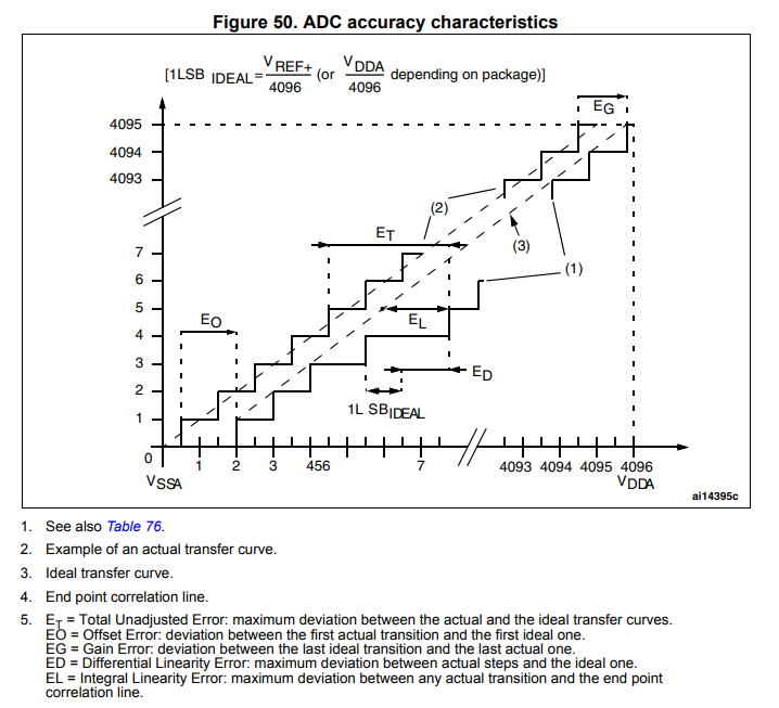
I believe it's all embedded in this graph from the device data sheet: -

enter image description here

So, calculate what 1 LSb means in terms of input voltage and multiply that by the digital value produced by that input voltage. You have to take into account several error factors though such as: -

  • Offset error (the input voltage equivalent to digital zero)
  • Gain error (the real average slope of the conversion line)
  • Integral non-linearity (the way in which the average conversion line might bulge a bit at extremes or in the middle).
  • Differential non-linearity (the imperfection in an input voltage change that brings about a digital change of 1 LSb).
\$\endgroup\$
0
\$\begingroup\$

Assuming ADC_Sample can only report values from 0-4095, then this formula:

V = ADC_sample / 4095 * 3.3

...is correct. Why? If you want to actually see 3.3V, you need to be able to achieve the second term:

V = ADC_Sample:4095 / 4095 * 3.3 = V = 4095 / 4095 * 3.3 = V = 1 * 3.3 = V = 3.3

If you used 4096 as the second term, you would never get 3.3...

V = ADC_Sample:4095 / 4096 * 3.3 = V = 4095 / 4096 * 3.3 ~ V = .999756 * 3.3 ~ V = 3.2992

Depending on how floating point rounds you may "see" 3.3 as a value there, but there are more errors in the middle.

\$\endgroup\$
1
  • 2
    \$\begingroup\$ Many ADC's can only go up to Vref-1LSB. If Vref is 3.3, the ADC has no code for 3.3V -- it is out of range. \$\endgroup\$ Commented Oct 7, 2019 at 15:39

Your Answer

By clicking “Post Your Answer”, you agree to our terms of service and acknowledge you have read our privacy policy.

Not the answer you're looking for? Browse other questions tagged or ask your own question.