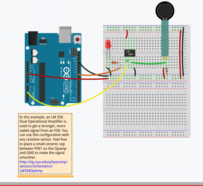
 I have this suggestion to a circuit I am developing
"place a small ceramic cap between PIN1 on the Opamp and GND to make the signal smoother."
Does the value of the capacitor make any difference?
Included the schema:
 I have this suggestion to a circuit I am developing
"place a small ceramic cap between PIN1 on the Opamp and GND to make the signal smoother."
Does the value of the capacitor make any difference?
Included the schema:
Pin 1 is the output of the LM358 op amp.
Adding capacitance to output of op amps is dangerous business because it can cause stability problems.
See what's in the LM358's data sheet:
Capacitive loads which are applied directly to the output of the amplifier reduce the loop stability margin. Values of 50 pF can be accommodated using the worst-case non-inverting unity gain connection. Large closed loop gains or resistive isolation should be used if larger load capacitance must be driven by the amplifier.
I do see that your circuit connects pins 1 and 2, which indicates the op amp is configured as a non-inverting unity gain configuration as mentioned in the paragraph above. Based on that, I would not go above 50pF.
I suggest you start placing a 33pF capacitor. If it doesn't bring any noticeable benefit to the integrity of the signal, just forget about it and don't run the risk of facing stability problems.
Lets suppose you want to drive an a ADC, at 100,000 Hz with 1 volt peak; suppose the total load current (DC + AC; steady plus charging current I == C * dV/dT == 2mA; we want the VDD supply to be steady +-1 millivolt so we have a good chance of millivolt opamp Vout cleanliness (Opamps cannot reject high frequency VDD trash, because the internal transistors are not given enough current to achieve that; thus its YOUR job to keep the VDD fairly steady by providing a capacitor).
Lets compute the needed capacitor. Start with Q = C * V, look for I == dQ/dT
I = C * dV/dT
C = I * dT/dV with I = 0.002 amps, dT = 10 microSeconds, dV = 0.001 volts
C = 0.002 amps * (1e-5 seconds / 0.001 volts ) = 2 * 1e-5 = 20 microFarads.
=====================================
Notice I don't show how to compute the Iout, the 2mA.
Your ADC likely has the behavior of grabbing a bunch of charge during the initial (start of every sample) Sample/Hold part of each conversion, to charge up the internal Sample/Hold capacitor. Expect the internal capacitor to be 5pF (its on the silicon surface, and big values require big silicon areas, which costs money) or maybe 10pF. And expect some resistance inside the ADC on the silicon, to limit the charging current. One volt and 1Kohm is 1mA; 2 volts and 1Kohm is 2mA, hence the 0.002 amp value I used.
Since your schematic does not specify the length of wires between your opamp and the power supply, I suggest you use the 20uF (use 22uF, or 33uF, or 47uF, or 100uF) within a centimeter of the OpAmp.
In this case, the standard 0.1uF probably will not produce a clean/steady Vout of the opamp, because we don't know the distance (the wiring length) between Opamp and Power Supply.
If you want to "smooth" the signal, the best place to put the capacitor would be on pin 3 of the opamp. In this location, it will function as an RC low-pass filter in conjunction with the effective source resistance of the voltage divider created by the FSR and the fixed resistor.