13
\$\begingroup\$

Silicon chips are made by slicing up wafers; in general, the fewer transistors a design needs, the smaller the area it needs, so the more chips you get out of a wafer, and the lower the cost per chip.

But there must be some limit to this. Maybe you can have a chip of one square millimeter area, but it seems unlikely that you could have a chip of one square micron area.

What is the minimum... To be specific, I'm not asking what is the minimum physically possible area, but what is the minimum area below which chips stop getting cheaper? The point at which you stop trying to shrink your design, because fewer transistors will no longer save money?

And has this remained roughly constant over the decades, or has it changed with iterations of process technology, and if so, in which direction?

\$\endgroup\$
4
  • 1
    \$\begingroup\$ I would imagine that the minimum area for a useful semiconductor is much bigger than the limit case you are asking to be considered. For practical marketing reasons nobody is going to design (say) a regular diode that burnt if the forward current exceeded 10 mA yet, there will be many many transistors on big pieces of silicon (a complex chip) that will struggle with a current as high as 10 mA. So, you need to focus your question some more to make it more practical for this site. \$\endgroup\$
    – Andy aka
    Commented Dec 30, 2019 at 13:51
  • 8
    \$\begingroup\$ The limiting factor is the chip dicer and practical smallest size for wire bond pads. \$\endgroup\$
    – D.A.S.
    Commented Dec 30, 2019 at 14:12
  • 3
    \$\begingroup\$ As a point of reference, a single transistor die that National Semi made was 0.381 x 0.381 mm. The transistor itself required a small portion, about the same area as the two bonding pads. \$\endgroup\$
    – glen_geek
    Commented Dec 30, 2019 at 14:16
  • 1
    \$\begingroup\$ As Tony implied you have to consider the I/O. Shrinking the die does not good if you can't get the number of I/O pins into the smaller size package. Also there is overhead of manufacturing so there is a point where the money saved by reducing becomes very small to the overhead cost and there is no gain in reducing die size. This is usually referred to as "The Point of No Return". \$\endgroup\$
    – jdweng
    Commented Jan 1, 2020 at 13:17

4 Answers 4

15
\$\begingroup\$

The minimum area of the chip is determined by the most cost effective solution not the smallest physical possible cut.

The smallest cut defect-free with a kerf is roughly equal to the wafer thickness and the slotted diamond saw roughly equal to 1/2 of the wafer thickness.

Thus the question should be what is the cheapest way to process single diode junctions. As the biggest demand for single diode junctions appears to be LED's , the question should be what is the maximum number of LED's per wafer? Economy has driven the size of the LED up. There is no benefit to going smaller.

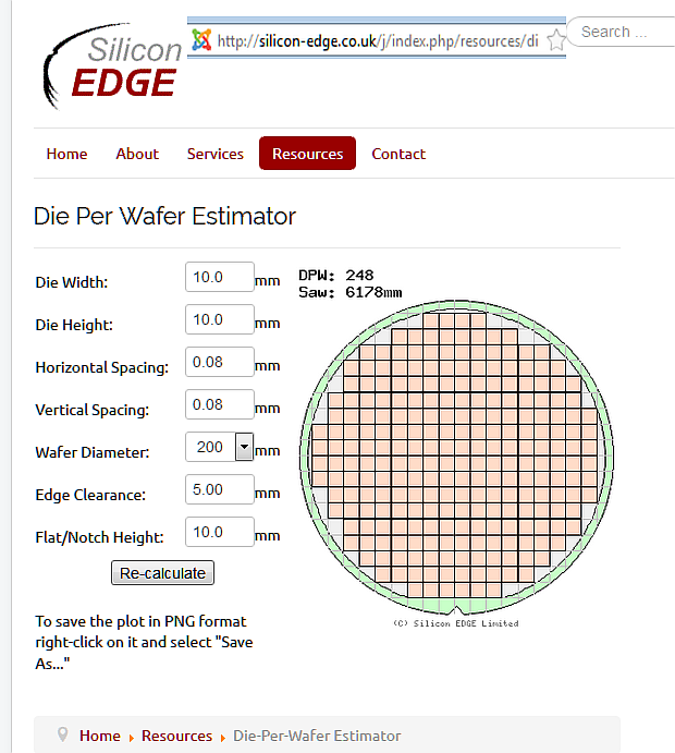
For any given chip on a die and wafer size, this calculation limits the maximum number of Die Per Wafer.

This is not the limit but is a calculator to determine the mechanical yield of a wafer.

enter image description here

The trend now is to make small flip chips with bump pads stacked on a system in package (SiP) or system-in-a-package with a number of integrated circuits enclosed in a single chip carrier package.

\$\endgroup\$
5
  • \$\begingroup\$ Isn't there a kerf on a chip dicer? \$\endgroup\$
    – DKNguyen
    Commented Dec 30, 2019 at 14:35
  • \$\begingroup\$ The defect free zone includes the kerf and saw width then add the street width margin to determine spacing \$\endgroup\$
    – D.A.S.
    Commented Dec 30, 2019 at 14:40
  • \$\begingroup\$ The size of LEDs has gone up for lighting, but microLED displays are pushing it the other direction. Not sure what state-of-the-art is, but definitely less than 20 μm on each side. Among the challenges for microLEDs, mechanically transferring these is a major issue in their development. \$\endgroup\$
    – IceGlasses
    Commented Dec 31, 2019 at 11:28
  • 1
    \$\begingroup\$ @IceGlasses "Each Sony CLED tile, dubbed ZRD-2, measures about 16 x 18 x 4 inches (WxHxD) and houses 320 x 360 pixels with a pixel pitch of 1.26mm. The tiles are mounted in a larger frame and laser-aligned to form a continuous, seamless screen" \$\endgroup\$
    – D.A.S.
    Commented Dec 31, 2019 at 15:27
  • \$\begingroup\$ @DKNguyen If using a saw for singulation, yes. If laser-dicing, not really. \$\endgroup\$
    – Shamtam
    Commented Dec 31, 2019 at 16:09
7
\$\begingroup\$

Chip costs are not die only.

There is testing, bonding, packaging etc.

You would be surprised how much time on a big chip tester costs!
Thus a chip with a small analog die with larger amount of test-vectors can be more expensive then a big digital one with fewer test-vectors.

\$\endgroup\$
1
  • 1
    \$\begingroup\$ As a ballpark rule of thumb, semiconductor production test time costs around a penny a second. \$\endgroup\$ Commented Jan 1, 2020 at 1:58
7
\$\begingroup\$

Even ignoring things like scribe keep-out margins, many IC designs end up being pad limited or bump limited given the IO required by the circuit (even capacitive IO coupling or antennas require some physical size). This is true not only for small chips, but many older larger chips had empty space because any smaller would not have allowed enough perimeter for the required number of IO pads (thus allowing room for free "chip art" on the die.)

\$\endgroup\$
3
  • \$\begingroup\$ Good point! What about e.g. the early 8-bit microprocessors like the 6502 and Z80, that had 40 I/O pads, what was the minimum space for them? \$\endgroup\$
    – rwallace
    Commented Dec 30, 2019 at 22:07
  • 3
    \$\begingroup\$ That is called 'pad limited'. If the core decides the size it is called 'core limited'. \$\endgroup\$
    – Oldfart
    Commented Dec 31, 2019 at 0:22
  • 2
    \$\begingroup\$ I remember using our SEM in the lab at Burroughs in Winnipeg to examine the chip of a Mickey Mouse watch in the 80's and we saw the cartoon character etched in silicon. "chip art" \$\endgroup\$
    – D.A.S.
    Commented Dec 31, 2019 at 16:31
4
\$\begingroup\$

Many posters mention bond pad size as a limiting factor. But some of our newer designs do not use wire bonds at all. The chip is built with bumps on the bottom that allow for direct chip attachment and connectivity to the substrate (board).

I think minimum die size has got to be determined by wafer dicing capability, and fallout (bad die) from that operation.

\$\endgroup\$
5
  • 1
    \$\begingroup\$ The "bumps on the bottom" still have a necessary size \$\endgroup\$ Commented Dec 30, 2019 at 15:19
  • 1
    \$\begingroup\$ The difference between bond pads and bump pads is just a matter of scale...either one is still enormous compared to the size of a transistor. \$\endgroup\$ Commented Dec 30, 2019 at 15:19
  • \$\begingroup\$ Agree with both the above comments. But bump pads on the bottom do not add to the periphery of the chip. Bump pads on a current design are 200 um in diameter, and are under a 10 mm x 10 mm die. \$\endgroup\$
    – SteveSh
    Commented Dec 30, 2019 at 15:39
  • 1
    \$\begingroup\$ @Elliot Alderson - depends on the type of transistor. If the transistor is part of a 7 nm design rules CPU, then yes. If the transistor is for an RF/microwave applications, probably not, particularly when the matching networks are included. \$\endgroup\$
    – SteveSh
    Commented Dec 30, 2019 at 15:51
  • 1
    \$\begingroup\$ I see a lot of wirebond pads in the 100x100 um range (or slightly smaller), so it seems if we're exploring the limits of die size, a wire-bonded chip (say a diode with two pads) can be smaller than a bumped chip. \$\endgroup\$
    – The Photon
    Commented Dec 30, 2019 at 17:31

Your Answer

By clicking “Post Your Answer”, you agree to our terms of service and acknowledge you have read our privacy policy.

Not the answer you're looking for? Browse other questions tagged or ask your own question.