2
\$\begingroup\$

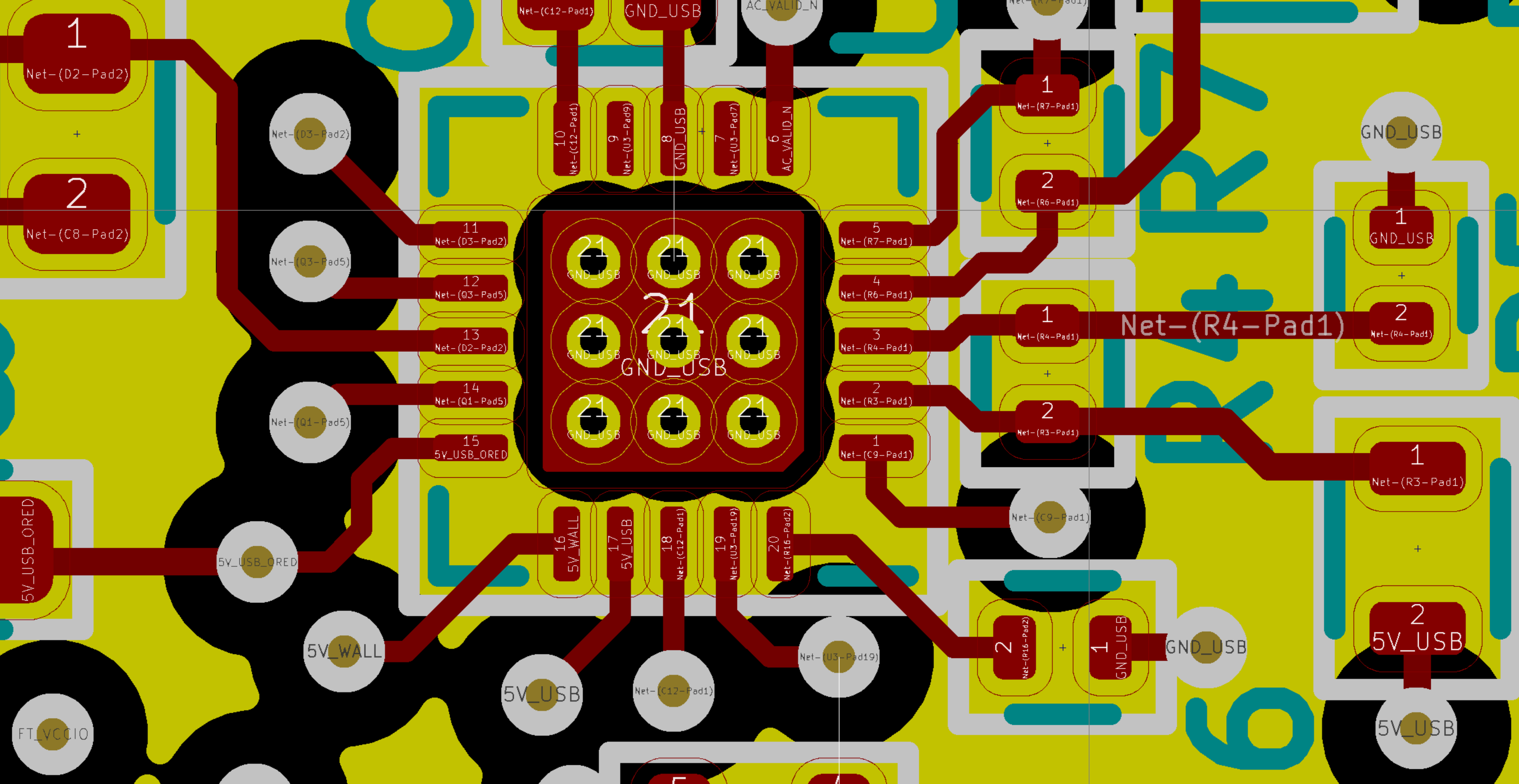
I am using KI-CAD. Visible in the picture is a GND_USB plane (yellow) on layer 2, and also the top layer (red). I have a QFN package with an exposed pad in the center. For some reason the ground plane won't flood into the thermal vias.

In the picture you can see that the ground plane floods over some other vias. It just won't flood over the ones that are part of the SMD footprint. In general I can't get zones to flood over any plated through holes in any footprints.

Each via in the footprint shows what net name is assigned to it from the schematic. They all say they are assigned to GND_USB (the same as the plane).

The vias are defined in the footprint as plated through holes, and exist on all copper layers.

What might be possible causes for why the ground plane won't flood over vias that are part of a footprint?

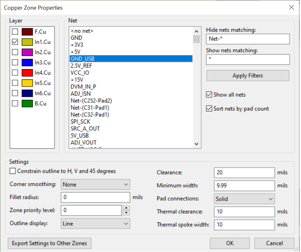
Note that the plane is staying exactly 20 mils from the vias, which is the clearance setting for the plane (zone). I confirmed this by reducing the clearance and watching the flooding get closer. So apparently the zone thinks it needs to maintain clearance from those vias even though they are the same net.

enter image description here

enter image description here

EDIT:

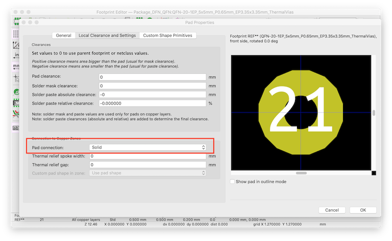
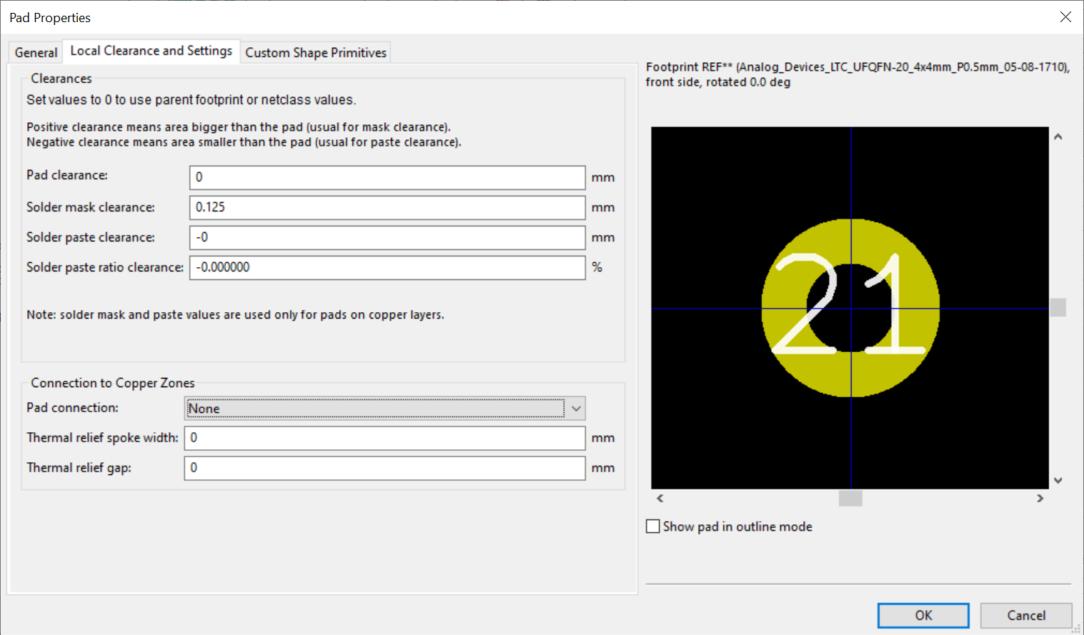
Well Seth found the setting. The problem was in the pad properties in the footprint. For some reason the "Pad Connection" property was set to "none" by default. I changed it to "Solid" and it works now. That was a little confusing because all the SMD pad types do connect by default so I never bothered to notice that setting. enter image description here
\$\endgroup\$
5
  • 1
    \$\begingroup\$ Just show a picture of the layer with the problem. Make invisible other layers. \$\endgroup\$
    – Andy aka
    Commented Jan 7, 2020 at 8:06
  • \$\begingroup\$ @Andyaka the problem is an interaction between one layer and the footprint which lives on another layer. I doubt seeing only the one layer would make the question clearer. What would help is seeing the footprint properties plus the pad properties. Sharing at least the footprint itself would reduce the work required and possibly make it even easier to answer. \$\endgroup\$ Commented Jan 7, 2020 at 16:06
  • \$\begingroup\$ It has to "live" on several layers for connectivity to happen @RenePöschl \$\endgroup\$
    – Andy aka
    Commented Jan 7, 2020 at 16:08
  • \$\begingroup\$ @RenePöschl The problem was in the pad properties. I added them to the question. \$\endgroup\$
    – user4574
    Commented Jan 8, 2020 at 4:35
  • \$\begingroup\$ The SMD pad you use here is a complex pad which does not support the normal default of "by parent" (because such pads do not support thermal spokes). So my guess is you created the large pad and then copied it or at least its settings to create the thermal vias. \$\endgroup\$ Commented Jan 9, 2020 at 1:45

2 Answers 2

5
\$\begingroup\$

The zone settings for your connection have a 10 mil clearance and 10 mil spoke width. This prevents the fill from being able to form a thermal spoke to the via. One way to adjust this is to change the settings of the thermal via pads to be solid connection like this:

Pad Properties

You will need to do this for all thermal vias in the footprint.

Alternatively, you can reduce the clearance size to smaller than the thermal via spacing in your zone settings.

-- Edit -- As Rene notes in the comments, you could also set this to (or leave it at) "From Parent" and ensure that the footprint Local Clearance and Settings is taking the connection type from the zone rather than forcing thermal vias.

\$\endgroup\$
4
  • 1
    \$\begingroup\$ Or set it to from parent which should mean that the zone settings are used \$\endgroup\$ Commented Jan 7, 2020 at 13:49
  • \$\begingroup\$ As "from parent" is the default it could also be that the footprint settings got changed to thermal instead of "from parent". \$\endgroup\$ Commented Jan 7, 2020 at 13:56
  • \$\begingroup\$ @Seth My use of the term "thermal via" may have been a little confusing but your answer led me to the solution. The engineers I work with typically use the term "thermal via" to refer to a via that is used to conduct heat away from a part. Those vias typically would not have "thermal spokes" or "thermals" on them since the spokes drastically lower the ability to conduct heat into the ground plane. We typically only use spokes when we intend to solder to the plated hole (for a through hole component lead). We typically just use "vias" to change layers or move heat and don't solder to them. \$\endgroup\$
    – user4574
    Commented Jan 8, 2020 at 4:33
  • \$\begingroup\$ Thermal via is the term we use in kicads official lib for the same things we see here. \$\endgroup\$ Commented Jan 9, 2020 at 1:43
2
\$\begingroup\$

Check your zone connection settings of your pads.

The large center pad of your footprint most likely is a so called complex pad (one made from a graphical polygon) These pads do not support the zone connection method of "thermals". Because of that the pad will default to zone connection "none".

My guess is that for some reason the small "vias" have the same setting.

\$\endgroup\$

Your Answer

By clicking “Post Your Answer”, you agree to our terms of service and acknowledge you have read our privacy policy.

Not the answer you're looking for? Browse other questions tagged or ask your own question.