2
\$\begingroup\$

I'm trying to build a stepper-motor driver. Each windig is driven as shown: H-bridge to drive one motor winding
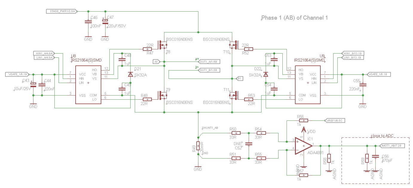
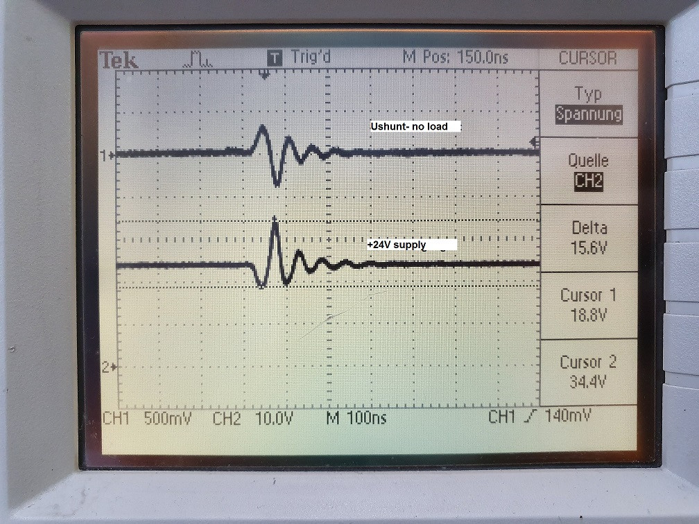
at the moment, im feeding this with PWNM signals of constant duty cycle, just to see how everything response. (PWMs are complementary to drive current in only one direcion) So i'm not using the OPAMP and MCU to measure any currents. What i see is that when a Mosfet gets turned on or off i see a spike over the shunt resistor, even with no load attached.

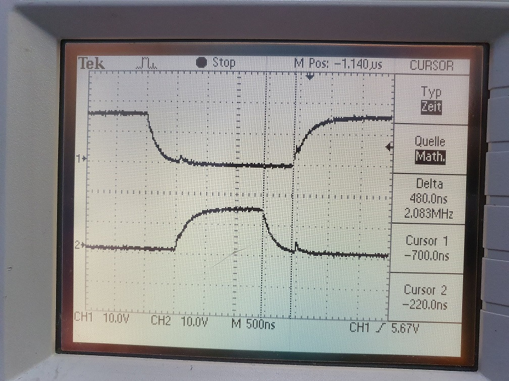
CH1 = voltage over shunt resistor CH2 = voltage at switching node

top: voltage over shunt (20mR) - bottom: output voltage close up on turn on

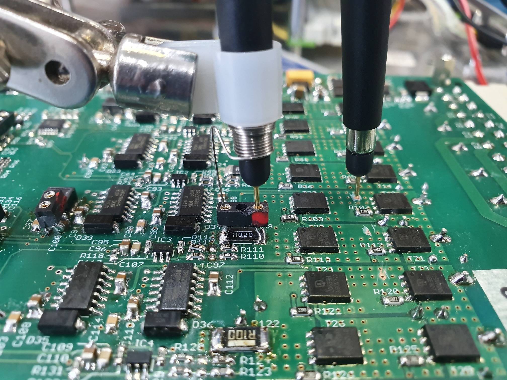
output voltage looks ok, same under load (testet with up to 3A). But im not shure where these spikes are comming from. I used a Ground-clip to measure this.

enter image description here

Any idea how i can get rid of this? Or is there anythin obvios wrong with my schematic. My current prototype uses a 4-Layer pcb with an (almost) solid GND-plane and seperate supply-planes under each H-bridge.

Update:

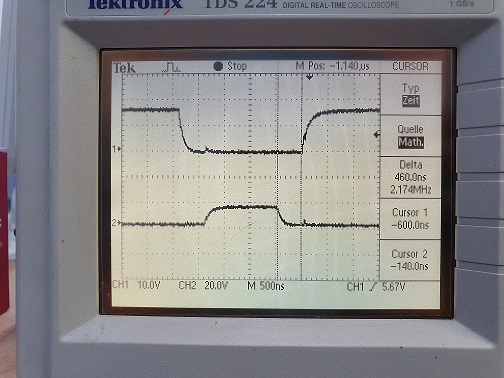
Dead-time of PWM signal is 460ns. I changed the gate resistors to 10R to allow for faster rise/fall of each gate voltage. but no improvment on the shunt signal

Output signal of the gate driver: enter image description here Gate voltages with RG = 22R enter image description here Gate voltages with RG = 10R enter image description here Better Measurement of gate voltages, might this peak be the problem? enter image description here
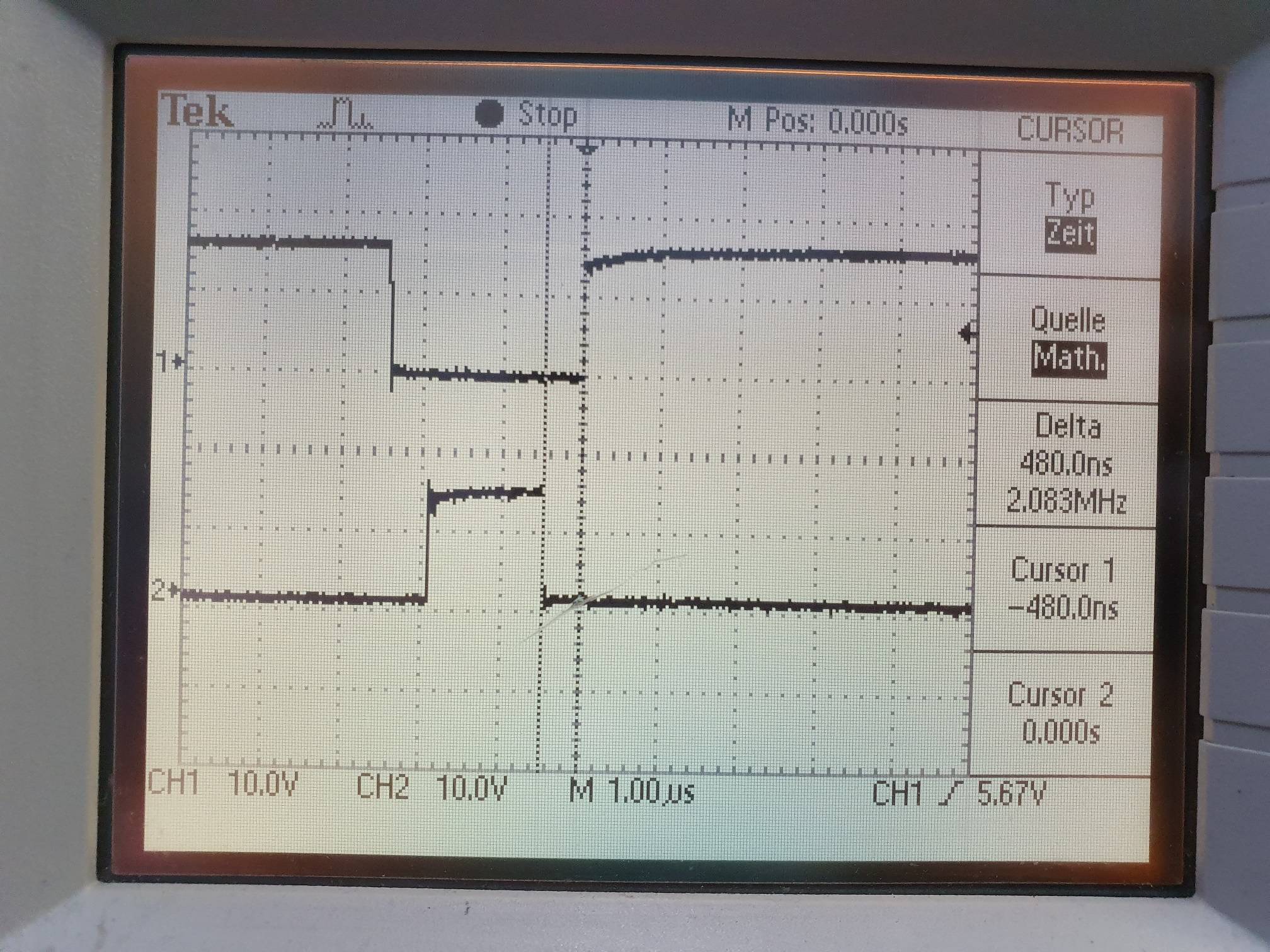
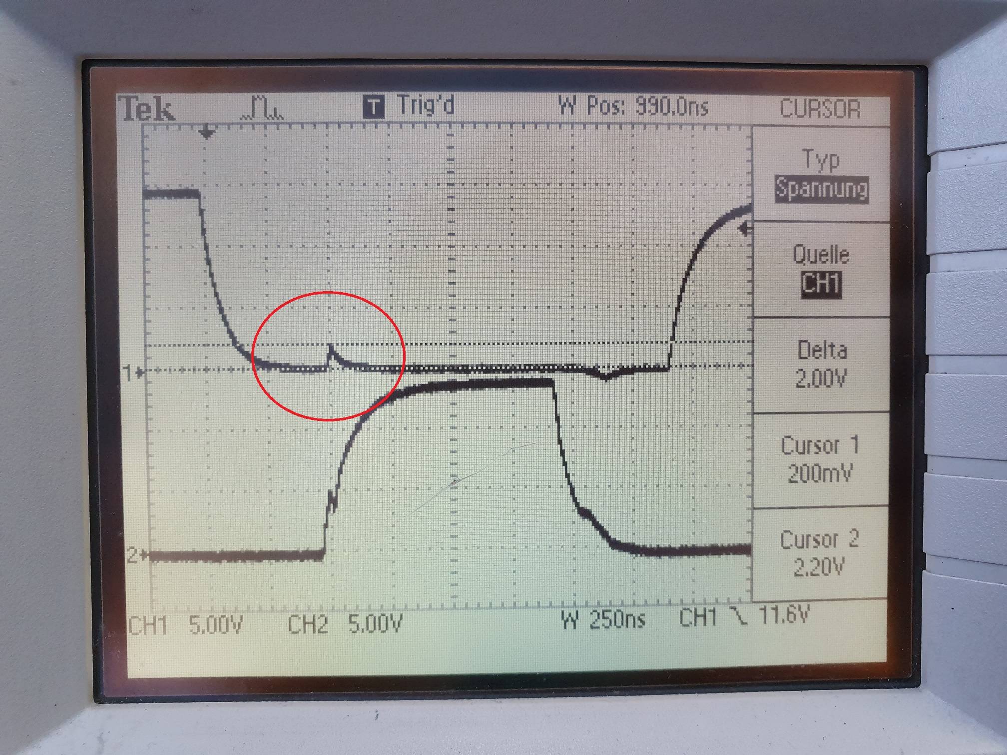
Update 2:

i've been testing and probing around to see if i can narrow it down. Wiring C49 and C54 directly to GND (as mentioned by peufeu) improved the signal over all, but it did not affect the spikes. But the signal is much cleaner right befor the spike, during dead time.

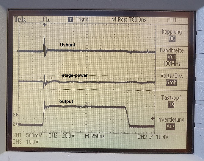
I found out that this Spike/swing is also present on the supply voltage. I changed C47 to 1000uF and still the supply voltage swings about +/-5V and more. Under no load, and there is no current drawn form the power supply. Wouldn't i take quite some current to cause such fast voltage change over an Elko? The swing on the supply voltage looks basically like the one over the shunt, but inverted.

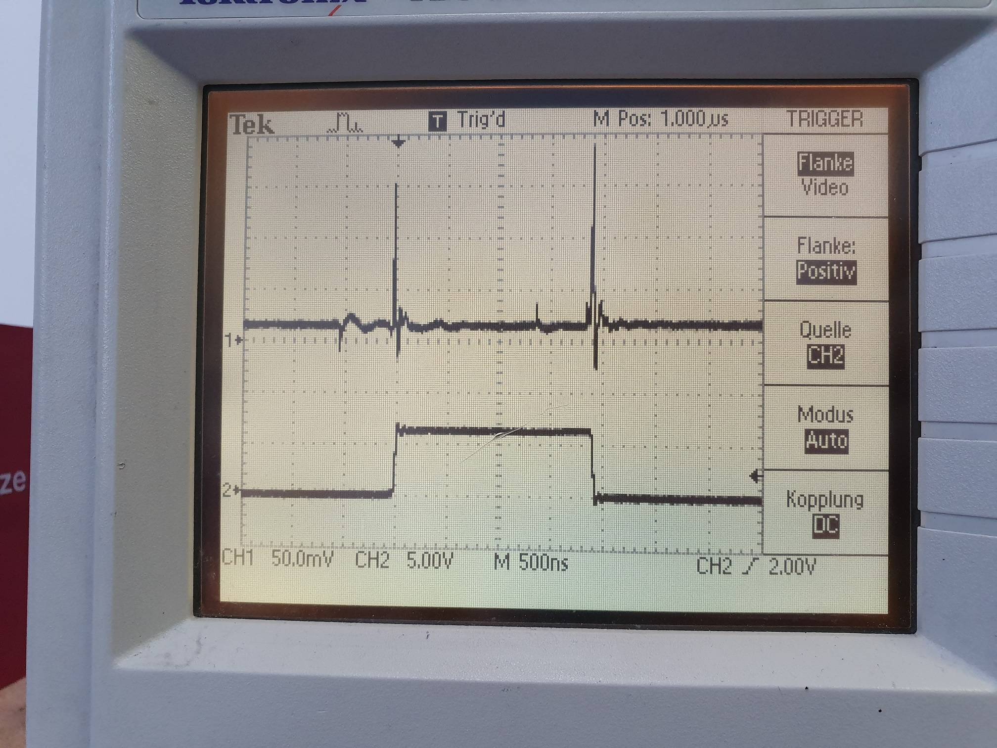
enter image description here enter image description here

\$\endgroup\$
6
  • \$\begingroup\$ Driver does have anti cross conduction feature, so both FETs can be ON at the same time. Try increasing dead time to a large value, so the turn-off of one FET and the turn-on of the other FET are clearly separated on screen. Does the spike on the current sense resistor occur at turn-off or turn-on? Is it the same for both FETs? (trying to narrow it down). Also maybe scope crosstalk between both channels? Try probing just the resistor, using only one channel. \$\endgroup\$
    – bobflux
    Commented Jan 21, 2020 at 17:18
  • \$\begingroup\$ i'm generating the PWM signals with 460ns dead time. Altough i noticed that if i measure after the gate resistor this dead time is nearly gone. i initially choose 22R as gate resistors to minimize ringing. I now changed this to 10R, ringing is still looking ok and both gate voltages ar now clearly separeted. Still no improvment on the shunt signal. \$\endgroup\$
    – mmarugg
    Commented Jan 22, 2020 at 7:11
  • \$\begingroup\$ "CH2 = voltage at switching node" by 'switching node' you mean the output, right? The fact that they are precisely aligned is a clue. Your FETs are rated for 30A on a typical PCB. What maximum current do you expect the load to draw? \$\endgroup\$ Commented Jan 22, 2020 at 9:10
  • \$\begingroup\$ Looking at the schematic I had missed that the VCC decoupling caps for the drivers, C49 and C54, do not connect to ground but to the positive pin of the sense resistor... That could couple switching noise from the driver into the current sense signal \$\endgroup\$
    – bobflux
    Commented Jan 22, 2020 at 10:15
  • \$\begingroup\$ with "Switching node" i mean the output voltage, Label out1_A or Out1_B. I intend to run phase currents of up to 4A over days. So i thought i go "big" on the FET to keep them cool in the long run. \$\endgroup\$
    – mmarugg
    Commented Jan 22, 2020 at 10:34

3 Answers 3

6
\$\begingroup\$

My first guess is that the newly activated leg of the H-bridge is starting to conduct before the leg being deactivated is fully off. Do you have any mechanism on the source signals to prevent overlap at the edges?

\$\endgroup\$
4
\$\begingroup\$

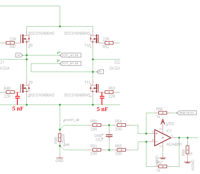
I think it might be worth considering the gate-source capacitance of your MOSFETs: -

enter image description here

They are nominally about 5 nF and I've added them on a portion of your circuit for you to consider. If you remove T8 and T10 you should be able to prove this. With T8 and T10 removed, if you still get the spike then it's gate capacitance passing the gate drive voltage through to the sense resistor.

It’s quite a common problem in some switch mode controllers and those that suffer from it use “blanking” techniques to avoid false over-current detection.

\$\endgroup\$
4
  • \$\begingroup\$ ok, so i removed T8 and T10. The spike generated by the turn-on of T8 is completely gone. I can still see when T9 turn on, but the peak is significantly smaller (like 75% less) i also tried to add aditional capacities between gate and source to worsen my signal, just to see if i'm on to something. But this doesnt seem to be the case. \$\endgroup\$
    – mmarugg
    Commented Jan 22, 2020 at 10:23
  • 1
    \$\begingroup\$ Well, if the spike with T8 and T10 removed is only 25% of the amplitude when T8 and T10 were in circuit then, it's more likely that the main body of the spike is due to a little bit of shoot-through. If you are familiar with simulators you should be able to narrow this down to the reason entirely without lifting a soldering iron @mmarugg \$\endgroup\$
    – Andy aka
    Commented Jan 22, 2020 at 12:11
  • \$\begingroup\$ i just noticed that there is a small peak on the low side gate voltage exactly when the high-side FETs starts conducting. This peak is about 2V high, which i think could be enough to cause short shoot trough. I'm not sure were this is comming from, but could this cause my problems? if so, any ideas for countermeasures? \$\endgroup\$
    – mmarugg
    Commented Jan 22, 2020 at 12:59
  • \$\begingroup\$ If the low side FET is off then, the spike seen on its gate when the high side FET turns on, is drain to gate capacitance (\$C_{RSS}\$ of circa 48 pF) injecting charge from the rapidly rising voltage on the drain. This is also a known about phenomenon. Lowering R48 and R53 will alleviate this providing that the driver can take that current surge. \$\endgroup\$
    – Andy aka
    Commented Jan 22, 2020 at 13:07
1
\$\begingroup\$

I found out that this Spike/swing is also present on the supply voltage... The swing on the supply voltage looks basically like the one over the shunt, but inverted.
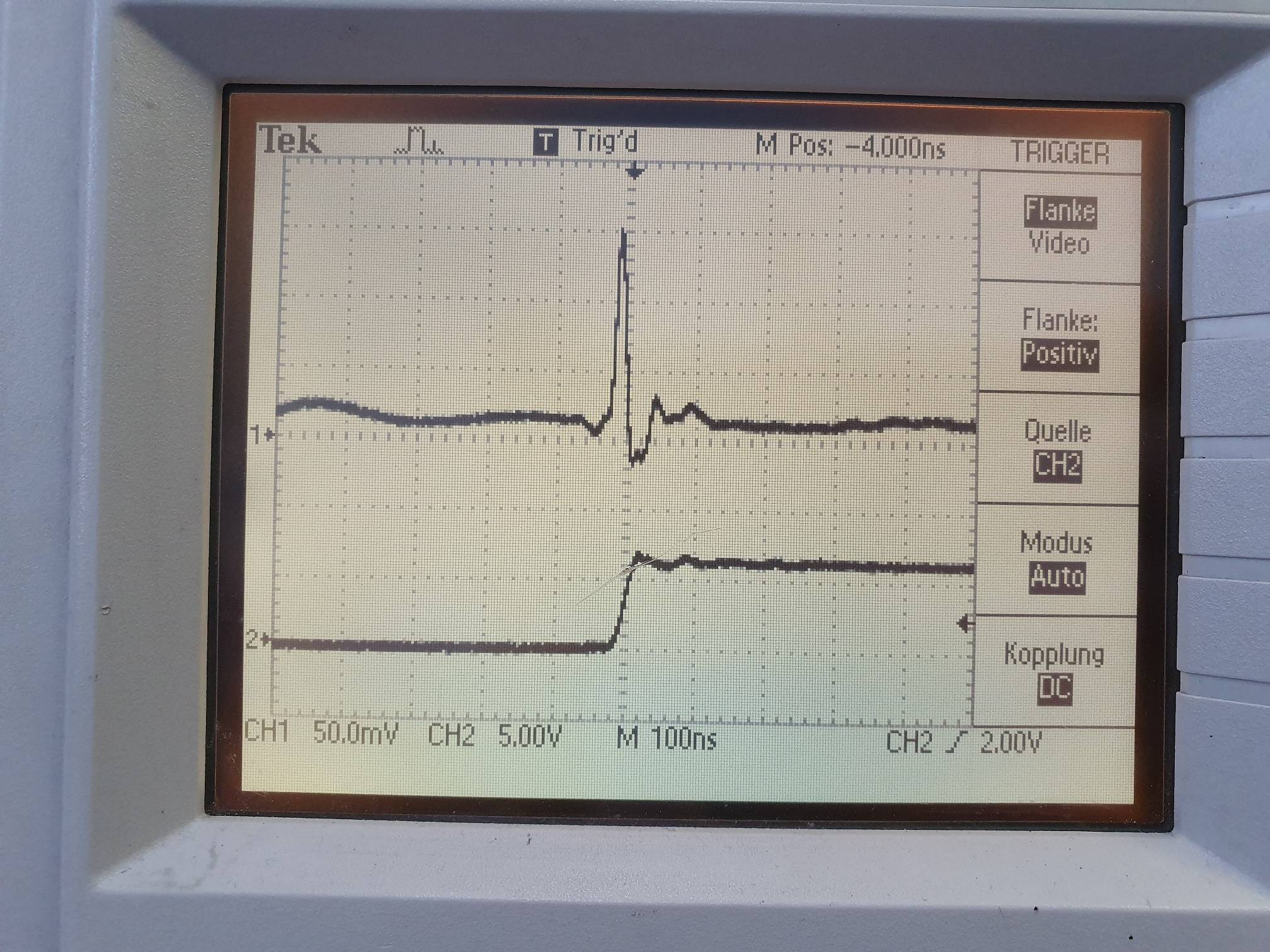
This is proof of current going through both upper and lower FETs rather than from lower FET Gate drive, but it is not 'shoot-through'. It is caused by Drain-Source capacitance, it's perfectly normal, and there's not much you can do to prevent it.

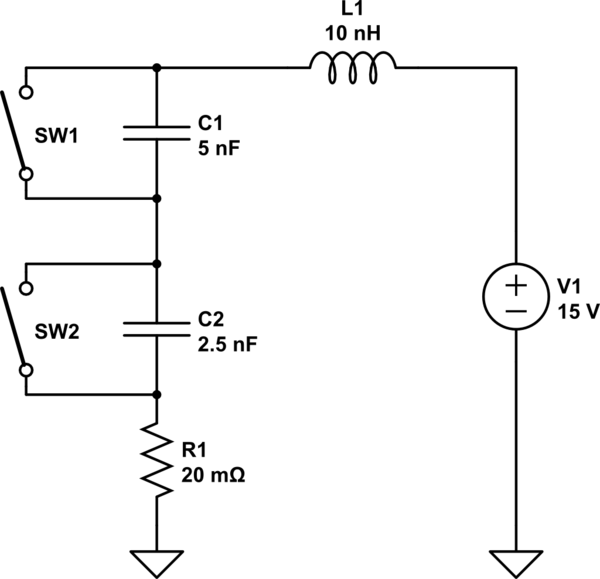
Your FETs have a Drain-Source capacitance of over 5 nF at 0V reducing to ~2.5nF at 15V, so a simplified equivalent circuit looks like this:-

schematic

simulate this circuit – Schematic created using CircuitLab

SW1 and SW2 are the upper and lower FETs, C1 and C2 are their Drain-Source capacitances, and L1 is the wiring inductance. Imagine that SW1 has just turned off so C1 is discharged. When SW2 turns on it causes C1 to charge via L1 and R1. This is effectively a series tuned circuit with (relatively) high Q, so instead of just charging C1 it rings at its resonant frequency.

The correct way to deal with this is hold off reading the shunt resistor voltage until after the switching surge is over. However a simple low pass filter will work if you don't need great accuracy.

\$\endgroup\$
1
  • \$\begingroup\$ i just checked this with an evaluation board from trinamic and i experience about the same noise. So as you said, seems to be normal. And under most conditions my current measurement is fast enaugh for the job. My FET are quite oversized, i may try some with lower Drain-Saurce capacity. - thank you for your help!!! \$\endgroup\$
    – mmarugg
    Commented Jan 28, 2020 at 10:46

Your Answer

By clicking “Post Your Answer”, you agree to our terms of service and acknowledge you have read our privacy policy.

Not the answer you're looking for? Browse other questions tagged or ask your own question.