2
\$\begingroup\$

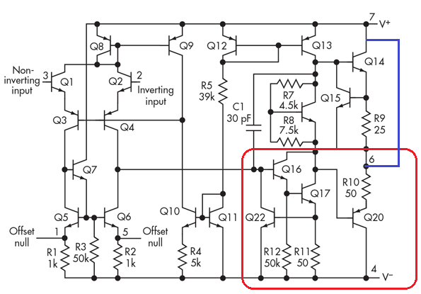
I have completed my answer to the question about the Widlar's limiting circuit but there is something unclear to me - how the transistor Q22 manages to limit the load current when the output is short-connected (in blue) to V+ or ground.

The usual explanation is that Q20 base current, entering Q17 and flowing through R11, increases sharply. As a result, the voltage drop across R11 increases as well, Q22 begins conducting and fixes Q16 base voltage.

But how is it possible somehow to change Q17 collector current while its base voltage is kept constant? Q17, like any BJT, behaves as a constant current source (sink here); so its collector current cannot be changed from the side of the collector... the voltage drop across R11 cannot be changed as well...

I have some explanation... but if it is true, I will not like this circuit solution so much... because it would not be valid in any case...

741 current limiter sink - shorted V+

\$\endgroup\$
6
  • \$\begingroup\$ But how is it possible somehow to change Q17 collector current while its base voltage is kept constant? - it isn't kept constant, Q22 reduces Q16's base voltage and that in turn reduces Q17's base voltage in order to "roughly" maintain a constant current through R11 (in turn that maintains approximately the same current into Q20's base). \$\endgroup\$
    – Andy aka
    Commented Feb 29, 2020 at 17:53
  • \$\begingroup\$ Q14, Q15 and R9 form a current limiter. For example , if the output is shorted to ground, the output current will be kept at Vbe/R9. \$\endgroup\$ Commented Feb 29, 2020 at 17:56
  • \$\begingroup\$ @Rohat Kılıç, I mean to consider the behavior of the lower current limiter (Q16, Q17 and Q22) when the op-amp output is short-connected to V+. \$\endgroup\$ Commented Feb 29, 2020 at 18:15
  • \$\begingroup\$ @Andy aka, Imagine, in the beginning, we have set some constant input voltage so that Q16 base voltage is constant. Then we connect a variable load resistor (rheostat) between the output and V+. There is some (small) Q20 base current that, together with Q13 quiescent collector current, enters Q17 collector. Both they flow through R11 and create a voltage drop that is unsufficient to turn on Q22. Then we begin decreasing RL up to zero (short to V+). Q20 base current increases... but Q17 (behaving as a current sink) shouldn't let it do that. So the voltage drop shouldn't change. \$\endgroup\$ Commented Feb 29, 2020 at 18:30
  • \$\begingroup\$ Circuit fantasist, You are right that the negative side of a current protection circuit won't work as efficiently as a positive side will do ( hard current limiting Vbe15/R9 = 30mA). Maybe this is why there is another version of this circuit righto.com/2015/10/inside-ubiquitous-741-op-amp-circuits.html used by Fairchild datasheet.octopart.com/LM741CN.-Fairchild-datasheet-7561151.pdf \$\endgroup\$
    – G36
    Commented Feb 29, 2020 at 19:31

3 Answers 3

7
\$\begingroup\$

I think I finally managed to unravel the mystery of the 741 sink (low-side) limiter... I will expose my guesses in the form of an imaginary story of how they were thinking when designing the circuit.

Original asymmetrical circuit solution

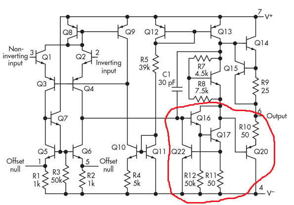
Sensing and limiting through the previous stage. In the initial 741 internal circuit diagram (Fig. 1), the Widlar's trick is applied only to the push transistor Q14 by Q15 and R9. For some reason (I will consider it below), it was unacceptable for it to be also applied to the pull transistor Q20. That is why they assigned the previous stage (the intermediate voltage amplifier Q16,Q17 and limiting transistor Q22) both to sense and limit the overcurrent.
741 initial sink

Fig. 1. In the initial 741 op-amp circuit solution, the previous stage both senses and limits the overcurrent

"Moving" the overload to the previous stage. The sensing is based on the properties of the BJT emitter follower. Let me clarify what this is about. In an emitter follower, the base-emitter junction makes a direct connection between the input and output. It is a one-way "diode" connection (from input to output). Under normal operating conditions, the transistor "lifts" its emitter voltage almost to the input base voltage level so that this direct connection does not work... and the base current is low (bootstrapping). When the output is grounded (short circuit), this phenomenon ceases to operate and the input is also grounded through the base-emitter junction... i.e., the overload is also applied to it. It would be not the case if the follower had been implemented with FET (source follower); so it is only valid for BJT.

No sensing the overload (ideal transistor). OK, the low load resistance is applied (through the Q20 base-emitter junction and 50 ohms R10) to the Q17 collector. And now the riddle comes into the picture, "How is it possible the load to change the Q17 collector current while its base voltage is kept constant? Q17, like any BJT, behaves as a constant current source (sink here); so its collector current cannot be changed from the side of the collector... the voltage drop across R11 cannot be changed as well.

(Practically, we have implemented this experiment as follows. In the beginning, we have set some constant input voltage so that Q17 base voltage is constant. Then we connect a variable load resistor (rheostat) between the output and V+. There is some (small) Q20 base current that, together with Q13 quiescent collector current, enters Q17 collector. Both they flow through R11 and create a voltage drop that is unsufficient to turn on Q22. Then we begin decreasing RL up to zero (short to V+). Q20 base current increases... but Q17 (behaving as a current sink) should not let it do that. So the voltage drop should not change.)

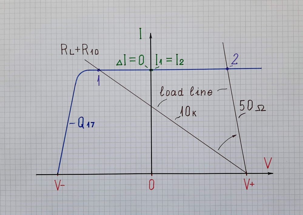
And this would indeed be the case if Q17 was an "ideal" transistor (without any Early effect) having an almost horizontal output IV curve - Fig. 2. When the resistance applied to the collector changes from RL + R10 to only R10, the load line rotates clockwise... the intersection (operating) point moves from 1 to 2 position... but the collector current does not change - I1 = I2, dI = 0. So the voltage drop across R11 does not change as well... and Q22 does not sense the overload.
741 sink limitier - Fig. 1

Fig. 2. Graphical solution of the circuit in the case of an "ideal" transistor (without Early effect)

There is even something else "harmful" here - the resistor R11 in the Q17 emitter introduces a negative feedback that tries to keep the current constant (emitter degeneration)... but, for the purposes of the overcurrent sensing, we want just the opposite...

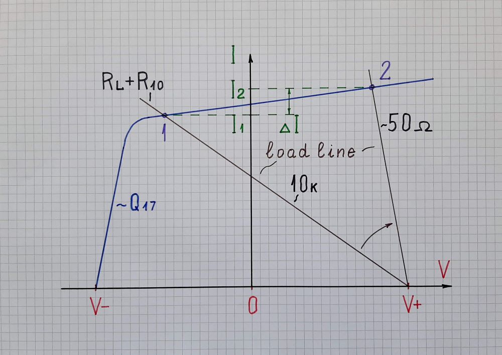
Sensing the overload (real transistor). But Q17 is a real transistor with Early effect and its output IV curve has some slope - Fig. 3. So when the operating point moves from 1 to 2 position, the collector current will (slightly) change from I1 to I2... the voltage drop across R11 will also (slightly) change... and Q22 should sense this change.
741 sink limitier - Fig. 2

Fig. 3. Graphical solution of the circuit in the case of a real transistor (with some Early effect)

The paradox of this idea is that, in order for this circuit to work well, the transistor Q17 should be poor... the poorer it is, the better Q22 will sense the overload. If Q17 is too perfect, Q22 may not sense it...

Never implemented symmetrical solution

However, the idea of a symmetrical current limiter in both output parts remains attractive. It can be found, for example, in the output stages of powerful amplifiers implemented by discrete elements - Fig. 4.
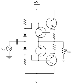
Push-pull amp protected

Fig. 4. Power amplifier with identical current limiters in both push and pull part

So why did not Widlar and designers at Fairchild do it in 741 op-amp? One possible explanation is that it cannot be done as @Jonk has said in the related question:

A symmetrically equivalent low-side isn't possible...

I made a lot of effort to figure out what the problem with this circuit was that it did not work. I turned my imagination into top gear (Fig. 5)... I even dug up old books from my student years... and still I have not found the reason... maybe simply because there was no principal reason for it not to work...
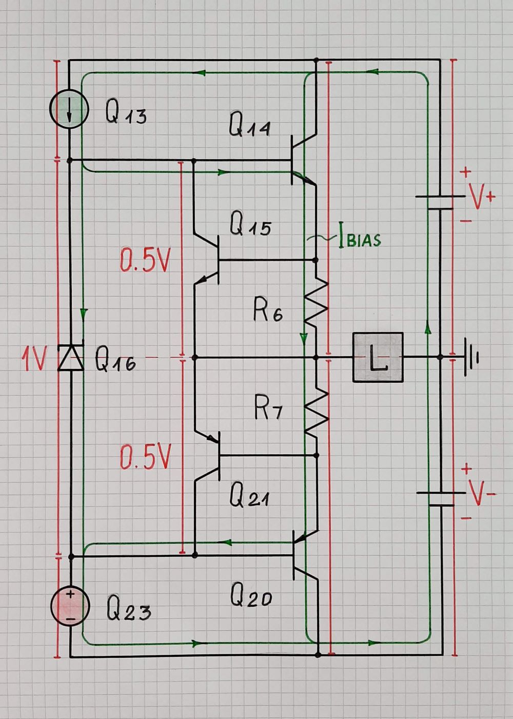
Can the symmetrical current limiter work

Fig. 5. Can the symmetrical current limiter work?

Apparently the circuit can work properly... but it works poorly... So I am more inclined to rely on @EinarA explanation above about the low performance of p-n-p transistors...

Improved symmetrical circuit solution

Maybe that was the reason that, in the next 741 version, the Widlar's followers from Fairchild separated the two functions so that the pull output stage senses while the previous stage limits the overcurrent (Fig. 6).
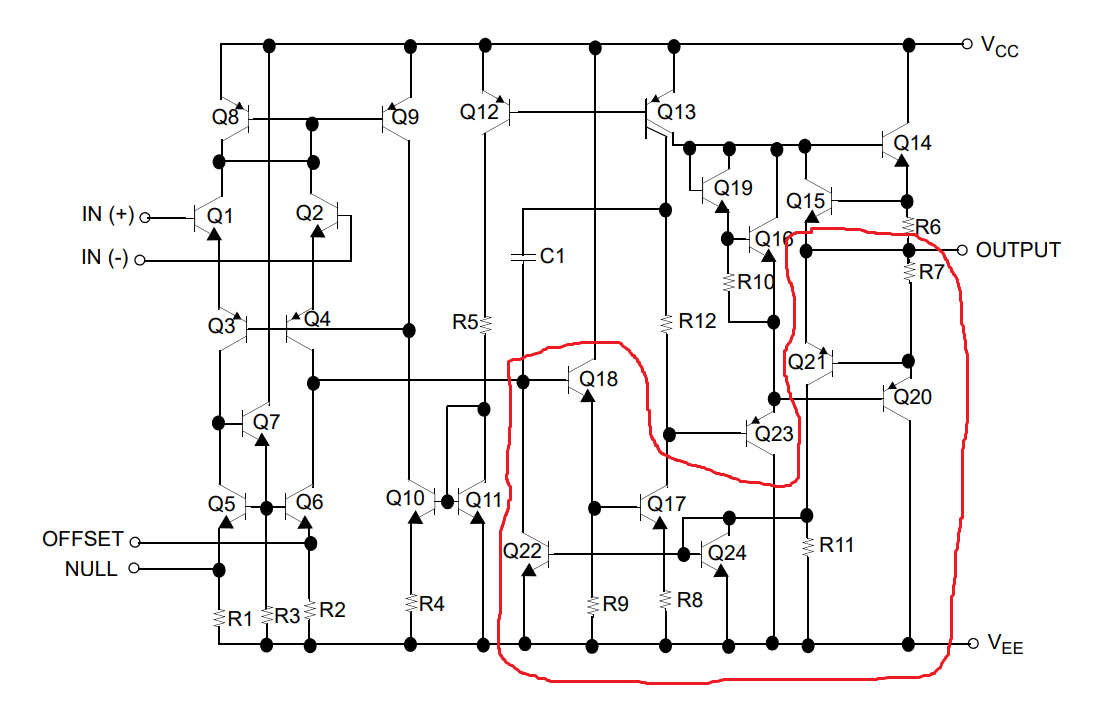
741 improved sink

Fig. 6. In the improved 741 op-amp, functions are separated - the pull output stage senses while the previous stage limits the overcurrent

It is done in the typical Widlar manner by connecting the low-side sensing circuit (Q21, R7) with the limiting transistor Q22 via a current mirror (Q22,Q24)... as though Q21 is moved at the place of Q22. The current mirror serves as a kind of "current transmission" connecting Q21 and Q22.

What is the benefit of all this? I think that thanks to the higher gain of the n-p-n Q22 and Q18, the current protection is triggered more sharply... and thus it is more efficient...

Is there a paradox here? No, now the transistor Q17 can be perfect as much as we want...

\$\endgroup\$
2
\$\begingroup\$

An essential point in understanding the behavior of this circuit is the low performance of Q20. The lateral PNPs of this era had a beta that dropped below ten at current levels of a few miliamps. So limiting current in Q17 will also limit current in Q20 to a reasonable amount. Later versions of the circuit used two diodes in series from the collector of Q17 to the output.

\$\endgroup\$
2
  • \$\begingroup\$ Two diodes - maybe to insert additional voltage drops in the path? There are too many drops along the current path from the short connection to ground. It seems there was a lot of reliance here on the imperfections of the elements for the purpose of the current limiting... \$\endgroup\$ Commented Feb 29, 2020 at 21:24
  • 1
    \$\begingroup\$ That is presumably why the diodes were added. The first version seems to assume that beta will be unity at 25 mA. This might not have always been the case, so diodes were added to give more control. \$\endgroup\$
    – EinarA
    Commented Mar 1, 2020 at 1:46
1
\$\begingroup\$

With output shorted to + supply, all the current from first stage Q8 current source flows towards the base of Q16 in a desperate attempt to pull the output down. Enough of this current flows into Q16's base to cause a big enough voltage drop across R11 sufficient to turn on Q22 which then diverts the rest of the current coming from the first stage to ground which limits Q20's collector current.

\$\endgroup\$
8
  • \$\begingroup\$ James, This is something new for me... So you assume that the voltage drop across R11 and turning on Q22 is implemented from the side of the input, not from the side of the output... as everyone claims? But does it depend on the load in the output? Will it not be the same as in the case of an open circuit (no load connected)? \$\endgroup\$ Commented Feb 29, 2020 at 18:36
  • \$\begingroup\$ The first stage is a transconductance stage (voltage in, current out). The voltage in is set by the difference between the op amp's inputs. When the output is shorted to +Vcc there will be a large difference between the inputs caused by the feedback network resulting in a large current out of the input stage. So the current out of the input stage is determined by what is happening at the output because of feedback. \$\endgroup\$
    – user173271
    Commented Feb 29, 2020 at 18:37
  • \$\begingroup\$ Well, but what if there is no feedback and the input voltages are such that the output is set to the negative rail? \$\endgroup\$ Commented Feb 29, 2020 at 18:44
  • \$\begingroup\$ So the question is, "How does the load current increase causes Q17 collector current increase... and, accordingly, R11 voltage drop increase... \$\endgroup\$ Commented Feb 29, 2020 at 18:51
  • \$\begingroup\$ At the risk of repeating myself (let me know if I'm getting boring), negative feedback causes a voltage difference at the input which pushes more current out of the input stage, driving Q17 harder. A larger load requires more current and so a larger voltage difference is needed at the input to supply the current. This means that there must be a small error voltage at the output to create the small required difference between the inputs. \$\endgroup\$
    – user173271
    Commented Feb 29, 2020 at 19:15

Your Answer

By clicking “Post Your Answer”, you agree to our terms of service and acknowledge you have read our privacy policy.

Not the answer you're looking for? Browse other questions tagged or ask your own question.