26
\$\begingroup\$

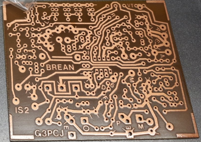
Regarding the attached PCB image, you'll notice that there are odd 'whiskers' from PCB pads. I'm curious as to their purpose.

PCB image

The board isn't high frequency, so I doubt it's for any fancy RF-magic.

My best guess is that because it is a home-etched board, these are intended to aid with component placement in the absence of a silk-screen layer: i.e., pointing out which way resistors go, etc., but there don't seem to be many places where components match.

Equally, it doesn't seem to match with another guess that they'd identify pin-1 on an IC or a common pin on switches, etc., so I'm at a bit of a loss.

I've never seen anything like it before. Any other suggestions welcome.

\$\endgroup\$
5
  • 5
    \$\begingroup\$ What is the purpose of this board? \$\endgroup\$ Commented Mar 6, 2020 at 13:22
  • 3
    \$\begingroup\$ Could it be a stylistic thing rather than serving a function? \$\endgroup\$
    – Colin
    Commented Mar 6, 2020 at 14:06
  • 1
    \$\begingroup\$ @WarrenHill it's some kind of radio circuit. Probably a HF transmitter/receiver at a guess. \$\endgroup\$
    – M1GEO
    Commented Mar 6, 2020 at 14:36
  • 3
    \$\begingroup\$ @M1GEO In your question you specifically state it isn't HF. \$\endgroup\$ Commented Mar 6, 2020 at 15:31
  • 9
    \$\begingroup\$ @evildemonic Sorry; yeah, I meant high frequency linguistically in the question (like GHz) and then by "HF transmitter" I meant in an terms of an engineering sense of <30 MHz. What I meant by when I said high frequency in the question was that these weren't a significant wavelength fraction of the operating frequency. Sorry for the confusion. \$\endgroup\$
    – M1GEO
    Commented Mar 6, 2020 at 15:57

6 Answers 6

25
\$\begingroup\$

Is there copper on the other side? If so, it's possible that these whiskers indicate that "vias" should be inserted in these holes.

I'm seeing two nets on the right labelled "A" (no whiskers) and "E" (all whiskers). Given there's an English ham radio callsign lower left, I'm guessing those are "Antenna" and "Earth" (the latter connecting to something on the other side, resembling a ground plane as far as possible on this style of PCB.

There used to be push in / snap off pins for this purpose (made by Harwin) though spare resistor legs, soldered both sides, are a perfectly acceptable substitute.

In fact, searching the callsign (plus BREAN) brings up the author's website where you can buy kits of slightly more recent manufacture. So why not email the author, and ask him?

Adding BREAN to the search term yields some hints that this may have been a DSB transceiver published in Practical Wireless - possibly December 2006 edition.

Re: comment. It's possible some of the supposed "all via" nets are either guard bands, or they might connect different islands of ground plane. Just a hypothesis at the moment.

OK there IS copper on the other side ... cross-referencing the tiny holes on the top of the board (without spot face cutter insulation rings) with the whiskered pads in the question, quite a lot of the traces match (I can't see every one)

As @DewiMorgan points out in a comment, these holes are ones where the top side copper hasn't been stripped. Some of these holes may be populated by a component leg, which should (if practical) be soldered both sides. Then it would be good practice to treat the remaining ones as vias (insert wire, solder both sides).

\$\endgroup\$
4
  • \$\begingroup\$ While I had come to the conclusion using Google, it doesn't answer the question. Take for example the long track along marked E. While I agree it makes sense to be earth, every pin on that track is ground stitched, so there's no space for anything else to connect to. Not even the antenna/power source!? An old packet BBS message says "Small 1.5W Phone DSB transceiver for 80m, or to 20m" so a DSB radio, 3.5 to 14.4 MHz. \$\endgroup\$
    – M1GEO
    Commented Mar 6, 2020 at 14:35
  • 2
    \$\begingroup\$ Looks like the dashes mean "copper has not been stripped back from this hole" - ALL the pins marked "topside solder points" in the document are dashed, and all the other dashed holes are the ones without the copper reamed away from the hole. \$\endgroup\$ Commented Mar 7, 2020 at 7:16
  • 2
    \$\begingroup\$ @DewiMorgan which is almost the same as "insert VIA here" ... I should refine it to "insert Via or component leg here". \$\endgroup\$
    – user16324
    Commented Mar 7, 2020 at 17:49
  • 1
    \$\begingroup\$ @DewiMorgan I assume this therefore means "solder on both sides of the PCB" which then bonds the track to the groundplane as a VIA would! \$\endgroup\$
    – M1GEO
    Commented Mar 8, 2020 at 21:22
13
\$\begingroup\$

No. This is a typical pcb from this UK supplier of ham radio kits. He has consistently made his boards with 1970s era Bishop Graphics, a sticky tape and donut system that became outdated with the advent of the first PC based design tools. But, being unwilling to adopt any other approach, he still supplies these woefully poorly hand drilled boards. They are generally double sided, the top side being unetched, forming an earth plane. Any ground circuit traces on the solder side have these 'whiskers tags to remind the builder to solder these leads on the top component side too. It's as awful a system as can be imagined, and makes building the kits very difficult, especially in the absence of overlay markings and with hand drawn circuits provided.

\$\endgroup\$
2
  • \$\begingroup\$ Thanks for the heads-up! I think that's basically what we concluded, but the backstory is entertaining! \$\endgroup\$
    – M1GEO
    Commented Mar 8, 2020 at 21:23
  • 1
    \$\begingroup\$ There are a few areas in your photo where holes are drilled in the wrong places (next to “D”), or the track doesn’t seem continuous (e.g. top left). \$\endgroup\$
    – David
    Commented Mar 9, 2020 at 0:07
9
\$\begingroup\$

These 'whiskers' seem to indicate that pads belong to a common net, probably 'ground'.

\$\endgroup\$
4
  • \$\begingroup\$ Definitely restricted to certain traces. Not sure about ground, have a look at the (presumably) DIP8 socket in the middle - not many ICs have ground only on that top middle pin (depending on how the board/IC are orientated!). \$\endgroup\$
    – awjlogan
    Commented Mar 6, 2020 at 13:10
  • \$\begingroup\$ @awjlogan DIP8 might be a switch not IC \$\endgroup\$
    – Peter MP
    Commented Mar 6, 2020 at 13:18
  • \$\begingroup\$ Indeed, could be anything really :) \$\endgroup\$
    – awjlogan
    Commented Mar 6, 2020 at 13:20
  • \$\begingroup\$ Might not be a common net, but an aid to etching. All whiskered pads are to be connected if they are close together. \$\endgroup\$
    – Sydwell
    Commented Mar 8, 2020 at 10:06
5
\$\begingroup\$

This is just pure speculation but your hint that it's a home-etched board (it does look manually drilled, and badly so) might point to the thin strips being indicators of over-etching.

\$\endgroup\$
7
  • \$\begingroup\$ I think you're on to something. I've never seen anything like it, even in my scalpel, tape and roundel PCB layout days (and this PCB definitely pre-dates CAD). As well as a "stop when they get too thin" signal, they may also help generate turbulence in the etchant (or even the stage before that, developing the photo resist) since they seem to be adding clutter in otherwise empty-ish areas. \$\endgroup\$
    – user16324
    Commented Mar 6, 2020 at 12:42
  • \$\begingroup\$ This is definitely a home-etched PCB, as the drill holes sometimes miss the centre slightly. \$\endgroup\$
    – M1GEO
    Commented Mar 6, 2020 at 13:59
  • 1
    \$\begingroup\$ @BrianDrummond I don’t miss using Bishop Graphics products one bit. \$\endgroup\$ Commented Mar 6, 2020 at 14:00
  • 1
    \$\begingroup\$ I'd have expected less consistency in the size and angling of the markings if they were overetched. \$\endgroup\$
    – Mast
    Commented Mar 7, 2020 at 11:02
  • 1
    \$\begingroup\$ @Mast my suggestion is that they could be deliberately added features used to indicate etching completeness. It may or may not be correct. \$\endgroup\$ Commented Mar 7, 2020 at 16:26
2
\$\begingroup\$

Looks interesting!

It might help with adhesion of the copper to the FR1 PCB. I imagine this pcb is single layered. These pads can break away from the pcb. With these "whiskers" it might be more robust.

\$\endgroup\$
1
  • \$\begingroup\$ Interesting. I notice that there are also some that don't physically connect to the pad, there are one or two that are just next to the pad. Perhaps those are indicating pin 1? \$\endgroup\$
    – M1GEO
    Commented Mar 6, 2020 at 14:12
1
\$\begingroup\$

These whiskers are only present in wider traces. Most probably these traces are ground net. The designer has just used these whiskers as markers for the ground traces.

\$\endgroup\$

Not the answer you're looking for? Browse other questions tagged or ask your own question.