1
\$\begingroup\$

I have a board that will take some 10 MHz clock lines and I was planning on surrounding said clock lines with ground traces to minimize interference with some other traces. I've been told to keep these ground traces about 30 mils from the signal line to reduce the capacitive load.

It is a 4 layer board, with two ground planes in the middle. My question is, should the ground trace connections also be connected to the ground plane? (This will happen through the same via where the connector is mounted to the PCB).

I'm aware that they are already technically shorted, since they are both sharing the same ground, but wanted to check if there was some reason why this is or is not a good idea (beginner at PCB design here).

Thanks

\$\endgroup\$
0

2 Answers 2

2
\$\begingroup\$

NoOOoooOOoOoooo. That's such a waste of a 4-layer PCB! Please find another approach than shorting two adjacent planes together to turn a very useful 4-layer PCB into effectively what is a 3-layer PCB.

That aside, there is also called a method called via fencing. It is like a ground ring, except in 3 dimensions where you tie parallel ground traces on layers above and below the signal trace with tightly spaced vias.

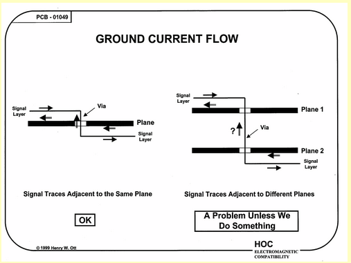
There is also potential issue which can arise whenever you have multiple planes. It is called changing reference planes. It is related to the fact that high frequency currents cannot flow through the copper plane due to the skin effect. They can only flow from one side of a plane to the other around the edges (such as the edges of via cutouts formed by signal traces as they pass through a plane).

enter image description here

Taken from: http://www.hottconsultants.com/techtips/pcb-stack-up-6.html

This is usually alleviated by placing ground vias near any signal via that passes through the plane, in order to provide a nearby edge for the return currents to cross from one side of the plane to the other.

But seriously, just read that entire link. The only reason I post the picture here is so the answer remains useful if the link ever gets broken.

\$\endgroup\$
2
  • \$\begingroup\$ Thanks a lot for the pointers. Will have a read of the link and see what I can learn. \$\endgroup\$ Commented Mar 31, 2020 at 15:12
  • \$\begingroup\$ @NathanBush That entire website is a gold mine, especially the Tech Tips section. I highly recommend his book. \$\endgroup\$
    – DKNguyen
    Commented Mar 31, 2020 at 15:14
1
\$\begingroup\$

Why waste both middle layers for a ground plane?

If you have ground traces on the board, especially lateral ones for shielding, they should be nailed to the ground plane at least every \$\lambda/20\$. If that's a square wave clock, the harmonics will go way above 10 MHz.

\$\endgroup\$
5
  • \$\begingroup\$ Is \$\lambda = c/f\$? If so \$\lambda = 3*10^8/10^7 = 30\$ meters is way beyond the pcb size hmm \$\endgroup\$
    – across
    Commented Mar 31, 2020 at 4:44
  • \$\begingroup\$ at the highest harmonic you want to consider? \$\endgroup\$
    – Neil_UK
    Commented Mar 31, 2020 at 5:02
  • \$\begingroup\$ The two ground planes just seemed convenient based on board symmetry, the manufacturing options I could find and that I wanted a ground right next to each of the signal lines. Agreed though, it's effectively a 3 layer board. Thanks for the comment, will look into it. They are square wave clocks but the pcb is only about 5cm long. \$\endgroup\$ Commented Mar 31, 2020 at 15:17
  • \$\begingroup\$ @NathanBush I would go S-G-S-[Power plane + component mounting] before I went S-G-G-S \$\endgroup\$
    – DKNguyen
    Commented Mar 31, 2020 at 17:49
  • \$\begingroup\$ I would go 1) component mounting and odd tracks, 2) ground plane, 3+4) Manhattan routed main routing, with ifnecessary, blind vias within the 3+4 layer. \$\endgroup\$
    – Neil_UK
    Commented Mar 31, 2020 at 20:27

Your Answer

By clicking “Post Your Answer”, you agree to our terms of service and acknowledge you have read our privacy policy.

Not the answer you're looking for? Browse other questions tagged or ask your own question.