1
\$\begingroup\$

this is my first post. I've been working on creating logic gates from 2N2222 transistors. I've build a basic switch, NOT Gate, OR, NOR, AND, NAND, and XOR (from a combination of the others). However, when I extend this to the XNOR, I get weird results.

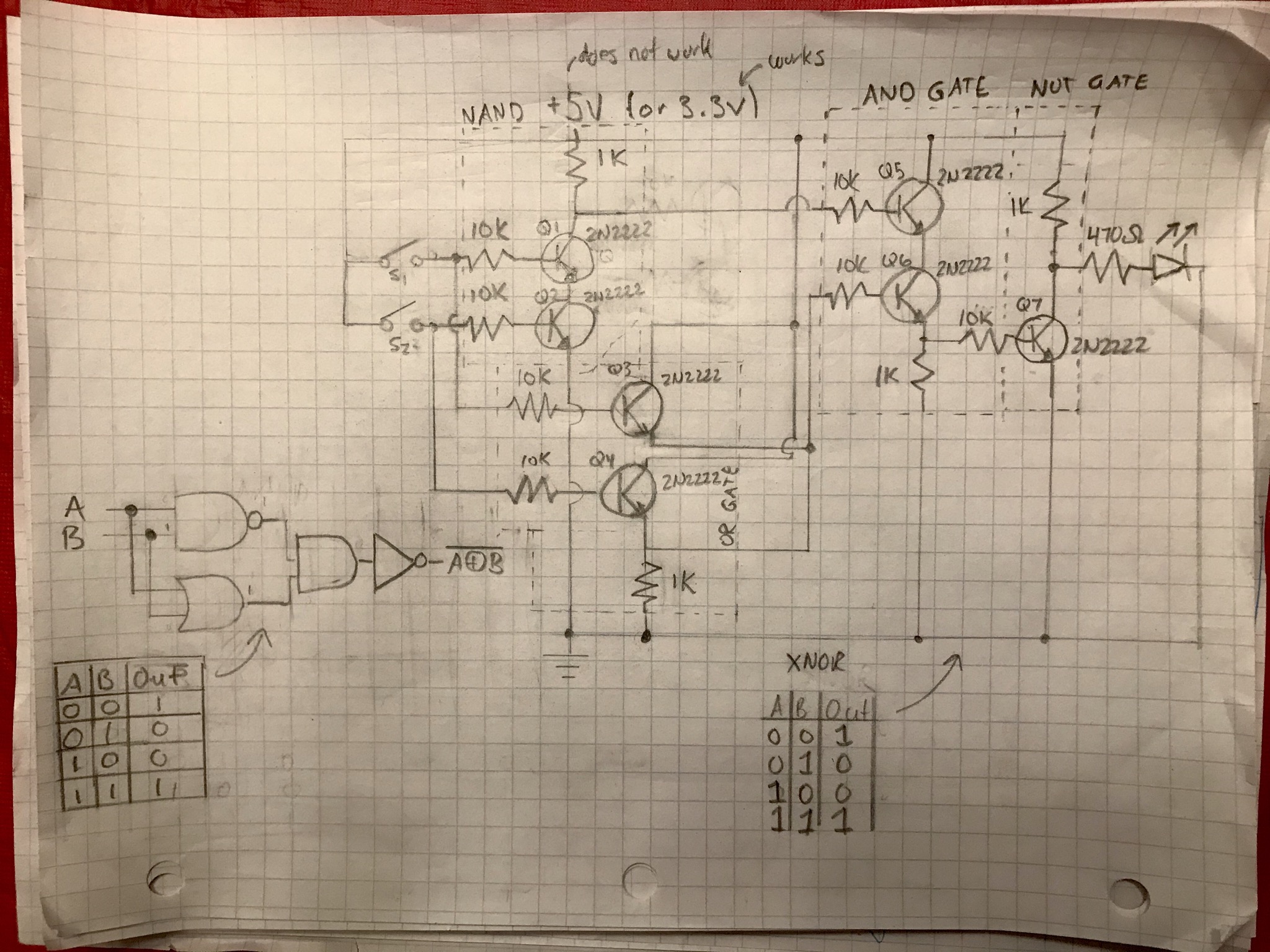
I started by building the circuit from NAND, OR, and AND, following this: http://hyperphysics.phy-astr.gsu.edu/hbase/Electronic/xor.html#c1. I then just wanted to add a NOT on the XOR output. I figured this was the best way to build up my knowledge from smaller parts.

When I run this with 3.3V, the circuit (blue or red LED lights up) follows the XNOR truth table. However, when I switch to 5V, I get weird behaviour:

  1. when both inputs are OFF, the LED is on, but not too bright (call this bright)
  2. when I turn one input ON, the LED dims; to be less than what I see in (1) (call this less bright)
  3. when I turn on the other input, it is the same as (2) (call this less bright)
  4. when I turn on both outputs, the LED is the brightest (call this brightest)

One of the first things I tried to debug this was connecting the output to a simple transistor switch that powers an LED. This works just fine. When XOR is ON, the transistor switch is on, and LED is on. When the XOR output is OFF, the LED is off. I then changed from the simple transistor switch to the inverter (NOT) gate and that's when I had issues.

I chose 10K for each base resistor, and 1K for the resistor either at Vcc or at Gnd. I chose 470ohms for the LED output (the LED is 3.0V to 3.2V and needs 20mA). I've tried changing the resistors at Vcc and Gnd to 4.7K to closely match the 5K that the link above showed. Again, this doesn't fix the issue.

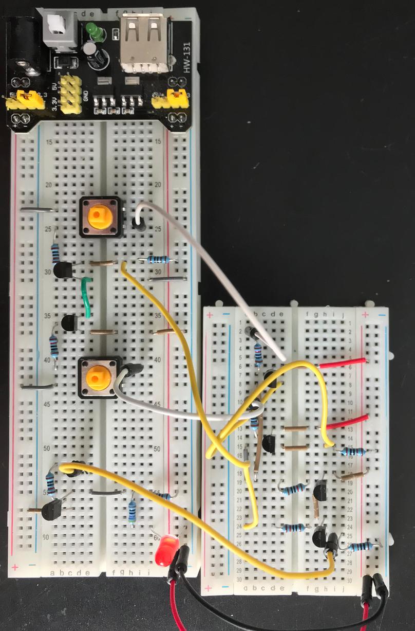
I have attached a picture to show the circuit. It isn't too clean, but I hope it helps. This shows the 3.3v setting, and this is when the circuit behaves as I would expect.

xnor at 3.3v

Edit: I hand drew the schematic. I’ll look into a schematic tool or the embedded editor next.
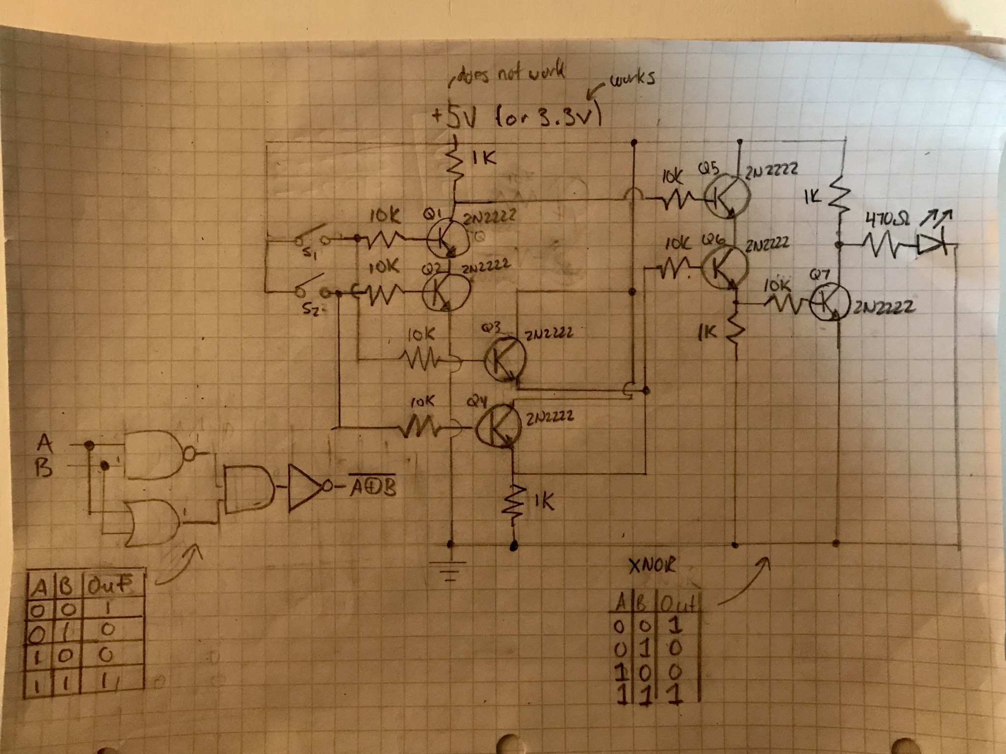
enter image description hereenter image description here

\$\endgroup\$
8
  • 1
    \$\begingroup\$ where is the schematics? \$\endgroup\$ Commented Apr 8, 2020 at 20:19
  • \$\begingroup\$ I don't have a tool for drawing schematics. I'd have to draw by hand. Alternatively, it should look like this the right hand diagram of the logic gate view on this page hyperphysics.phy-astr.gsu.edu/hbase/Electronic/xor.html#c1 where the output is connected to the circuit here hyperphysics.phy-astr.gsu.edu/hbase/Electronic/buffer.html#c3. I can try to find a tool or draw by hand. Just need some time. \$\endgroup\$
    – SteveB
    Commented Apr 8, 2020 at 20:46
  • 1
    \$\begingroup\$ When editing your question, you can click the schematic icon and get an in-browser schematic editor. \$\endgroup\$
    – The Photon
    Commented Apr 8, 2020 at 21:05
  • \$\begingroup\$ Or, hit ctrl-m, and that will also get you into the schematic editor. \$\endgroup\$ Commented Apr 8, 2020 at 22:03
  • \$\begingroup\$ I think Q5 and Q6 make a bar AND gate. Any base current into Q6 will pass through to Q7 and turn it on a bit. See if my answer to electronics.stackexchange.com/a/481942/73158 helps. \$\endgroup\$
    – Transistor
    Commented Apr 8, 2020 at 23:33

1 Answer 1

2
\$\begingroup\$

Please review my RTL NOR answer provided a while ago for detailed design and simulation information about RTL gates. In particular, the dual-stacked BJT form of a NAND gate as shown in your drawings is crap. I'm not going to belabor the details why, here. I'll just let you learn from experience on that one, for now. We've other fish to fry.

If you look at the Apollo Guidance Computer Schematics from many decades ago when RTL was used, you'll essentially one and only one kind of gate being used: NOR. There's a good reason for this and you can first read through my RTL NOR answer thoroughly and then attempt to design an equivalent 1-BJT NAND or AND or OR gate and see how well you fare at the problem.

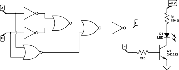
If you want to make a reliable, well-designed XNOR out of RTL, you can do this with six transistors (plus one to buffer your LED and maintain the "sense" (ON when XNOR output is HIGH and OFF when XNOR output is LOW.)

schematic

simulate this circuit – Schematic created using CircuitLab

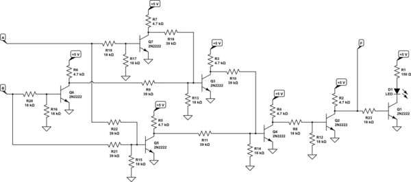
Using the design from my RTL NOR answer, you'd find the following schematic:

schematic

simulate this circuit

That circuit will work fine as an XNOR. And it will do so within managed specifications, too. 21 resistors, with only two different values, and 6 BJTs (only NPNs) for the XNOR. Plus another BJT and 2 resistors and LED for the display output. Probably about \$4-5\:\text{mA}\$ when the LED is OFF and perhaps \$25\:\text{mA}\$ with the LED ON. So, as an XNOR gate itself (no LED) it dissipates about \$100\:\text{mW}\$.

(The inverters above can be further minimized (but with some loss of management) by removing their input pull-downs. But I'd prefer you keep them in place.)

\$\endgroup\$

Your Answer

By clicking “Post Your Answer”, you agree to our terms of service and acknowledge you have read our privacy policy.

Not the answer you're looking for? Browse other questions tagged or ask your own question.