0
\$\begingroup\$

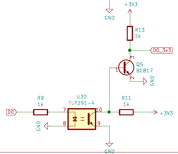
I have this circuit that is part of a schematic that I am trying to read. I have some idea, but I am not sure that I am correct. All I want is to figure out the D0 and D0_3V3 values.

For example assuming that the circuit that is connected to left D0 is set to low (no voltage), will D0_3V3 will be 0 (low) or 1 (high)? (I don't care for real measurements as this is either high or low, as if this is on a micro-controller circuit will get voltage or not.)

The bottom part with the R11 and +3V3 gets me confused as it seems to keep the NPN transistor always on, which it cant be. And if the NPN is always on then there's always high signal at D0_3V3?

Thank you very much all and sorry for making a such a newbie question!

enter image description here

\$\endgroup\$
3
  • 1
    \$\begingroup\$ R11 should be oriented in the same direction as R13 ... that would make it very clear at a glance that R11 is a pullup resistor \$\endgroup\$
    – jsotola
    Commented Apr 22, 2020 at 19:36
  • \$\begingroup\$ That is one ugly schematic. The grounds should all be pointing down, +V supply voltage arrow should be pointing up, and R11 should be placed next to R13 and connected together with it. No wonder a beginner has a hard time connecting the dots. \$\endgroup\$ Commented Apr 22, 2020 at 19:44
  • \$\begingroup\$ Thank you both! The R11 change of direction would indeed make it more clear! For sure helped me a lot ! Thank you again! \$\endgroup\$ Commented Apr 22, 2020 at 19:55

3 Answers 3

1
\$\begingroup\$

For example assuming that the circuit that is connected to left D0 is set to low (no voltage), will D0_3V3 will be 0 (low) or 1 (high)? (

D0 LOW

  • If D0 is LOW then the LED will be off and the photo-transistor will be off (high impedance and no current between the collector and the emitter).
  • Pin 10 will be pulled high by R11.
  • Q5 will be turned on.
  • D0_3V3 will be pulled LOW.

D0 HIGH

  • If D0 is HIGH then the LED will be on and the photo-transistor will be on (low impedance, and current will flow between the collector and the emitter).
  • Pin 10 will pull Q5 base to ground.
  • Q5 will be turned off.
  • D0_3V3 will be pulled HIGH by R13.
\$\endgroup\$
1
  • \$\begingroup\$ Thank you. Very detailed explanation. I think i understand it now. And thank you for editing my post also. I will remember your corrections and learn from them. \$\endgroup\$ Commented Apr 22, 2020 at 19:57
1
\$\begingroup\$

Both the optocoupler and the NPN invert the signal, so zero in is zero out, high in (with enough current) is high out. When the optocoupler turns on (on a high input), it grounds the base of the NPN, stealing its drive current and turning it off, allowing 3V3 to be pulled high.

\$\endgroup\$
1
  • \$\begingroup\$ Thank you. Actually i got a bit from every answer and helped me really a lot! \$\endgroup\$ Commented Apr 22, 2020 at 20:00
0
\$\begingroup\$

The bottom part with the R11 and +3V3 gets me confused as it seems to keep the NPN transistor always on, which it cant be. And if the NPN is always on then there's always high signal at D0_3V3?

There are a couple of things wrong with these statements.

1) First if the NPN (Q5) is always ON, it pulls DO_3v3 to GND.

2) Q5 is only on if the opto is OFF. If the opto is turned ON then Q5 is OFF also, since the base voltage on Q5 is ~0V.

\$\endgroup\$
1
  • \$\begingroup\$ Thank you. Yeah, i see the false on my thought now. As it seem i had no real understanding about how the DO_3v3 works. \$\endgroup\$ Commented Apr 22, 2020 at 20:02

Your Answer

By clicking “Post Your Answer”, you agree to our terms of service and acknowledge you have read our privacy policy.

Not the answer you're looking for? Browse other questions tagged or ask your own question.