I do these types of layout using Eagle. But any PCB layout software should work.
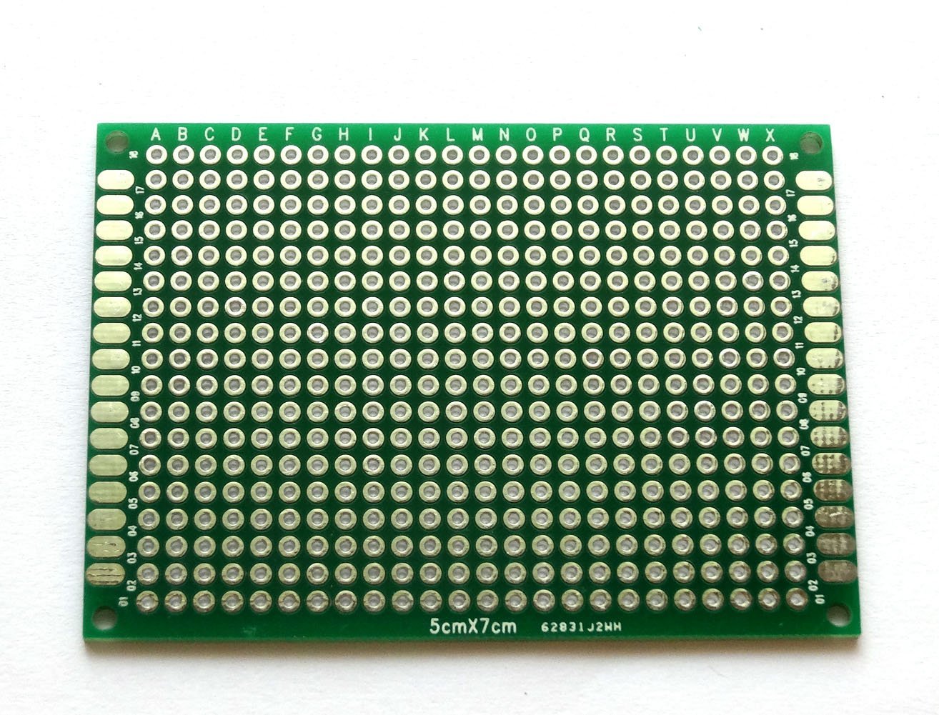
I set the grid size to 0.1” to match the pitch of the protoboard through holes. At each point the grid lines cross is where a through hole would be on the protoboard. You can then align your components’ pins to match those points.
You then run traces making sure to stick to 90 degree bends. If your protoboard is two layer, you can use both TOP and BOTTOM layers in Eagle, which makes it clear which traces go where.
For single-sided protoboards I use the TOP layer to draw jumper wires. Again, makes it very clear.
This also works for strip/veroboard but you’re obviously limited to horizontal traces. I layout the components and then draw in the horizontal traces where they need to go. This helps show where you need to break the tracks.
It can be a little bit of a faff to setup, but works great once you get going. Using Eagle or similar means you can take advantage of the rats nest tool to make sure you’re not missing any connections.
Update
Pictures always make things better, so here we go:

This image shows the layout. You can see the grid, with the intersections being the through holes. All the parts are aligned to this. Blue traces are the Bottom layer. Red traces are the jumpers on the Top layer.
In the past I have tried to minimise jumpers etc, but you could spend hours and hours trying to get everything on one layer. Plenty of jumpers give you more places to use as test points!
What is a good idea is to space things out as much as you can. It makes things much easier when soldering, and gives some wiggle room for on the fly adjustments - or for bodging down the line!

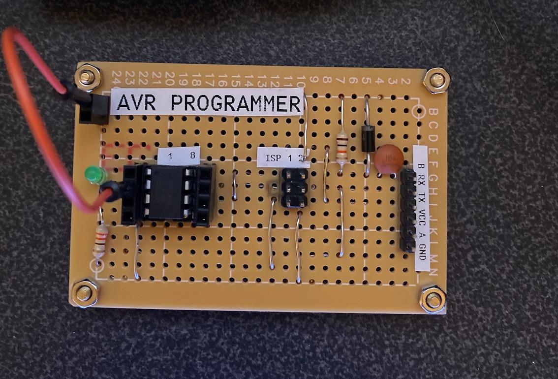
This second image is the final result. I don't have a picture of the bottom, but it more or less matches the board layout in the first image.
The LED arrangement is slightly different, as I adjusted this on the fly.


