4
\$\begingroup\$

I'm trying to understand how biasing works in ICs. When using discrete transistors we are told to bias them using polarization circuits typically made of voltage dividers. Then ac signal is introduced with coupling capacitors. However, in analog IC textbooks we are told that bias is done with current sources. The problem with this, is that I cannot understand how DC voltages are set in this scenario, and why are ac signal sources connected directly without coupling capacitors.

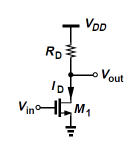
For example, in the circuit shown in the picture below. I assume that Rd is supposed to represent a current source that forces ID to flow into the transistor, but then how is the DC voltage at the gate set ? Moreover, why in most analog IC textbooks no coupling capacitors are shown when adding the ac signal source? Are they not used at all in ICs ? How can this be possible ?

enter image description here

\$\endgroup\$
2
  • \$\begingroup\$ "RD is supposed to represent a current source"...No - that is not the right understanding of the working principle. In this case, the current through the transistor would be nearly constant. But the opposite is true: The transistor acts as a (non-ideal) current source....and this current is controlled by the gate voltage. \$\endgroup\$
    – LvW
    Commented May 5, 2020 at 7:53
  • \$\begingroup\$ To bias this amplifying stage means to set Vout in the middle of the supply range (Vdd/2). For this purpose, you can connect a variable bias voltage source to the input (gate-source) and adjust its voltage so that Vout = Vdd/2. Then you have to insert the input voltage source in series to the bias source. One of them will be floating... and this is the main problem when biasing. Look at my answer below where I have tried to explain in simple words how to solve it... \$\endgroup\$ Commented May 5, 2020 at 20:03

5 Answers 5

3
\$\begingroup\$

The biasing is not shown in your figure. You should assume that the DC part of Vin does the biasing. In textbooks and higher level diagrams it is often omitted to reduce the clutter and make it easier to focus on the important parts. RD is only a load which sets the gain and DC voltage at the output (Vout= Vdd - Id*RD)

What is biasing? Setting the device in the required ID(VGS) point. You can either force a current through the device, which sets the VGS as well, or you force a VGS to the device which in turn generates the ID.

Biasing: voltage or current?: Even with discrete devices, the biasing through current would be better. Why? Reduced sensitivity to biasing error and noise. The current is a very strong function of the voltage (quadratic or exponential), which means that a small change in the input voltage induce a much higher relative change in the current. If current bias is used and there is a small error in the current, the error in the voltage would be even smaller in relative terms.

The only reason why discrete designs does not use current to set the bias point is due to the additional cost and area of current generation and current mirrors. These things are basically free in an IC design.

Also the variations (process or mismatch) in the threshold voltage (MOS case) would lead to output currents varying more. Using an existing current reference and a current mirror, it is possible to cancel out these and other changes in the transistor parameters (Cox, mobility, threshold voltage, temperature, etc.). Also in most of the cases sending current through the chip is more resistance to noises or ground bounce. (There are cases when sending a voltage makes more sense.)

AC coupling: It requires a big floating (=one side is not grounded) capacitor with high quality factor, and low parasitics towards other nodes (mainly ground). Such a thing does not exist in audio frequencies, and it becomes meaningful at higher frequencies.

Note that resistors in general are not welcomed in IC design. They are bulky and aren't precise. Everywhere where it is possible, active loads are used. It is smaller and provides a higher gain.

\$\endgroup\$
5
  • \$\begingroup\$ There are interesting thoughts (compared to the usual banal explanations) in your answer... IMO "higher level diagrams" and reducing the clutter" usually reduces the chance of understanding. It is interesting to explain how we can "force a current through the device" which has the property to keep the current constant... \$\endgroup\$ Commented May 5, 2020 at 20:22
  • 1
    \$\begingroup\$ @Circuitfantasist Thanks for the comment. They are good points. These expression meant to highlight, why the biasing is not shown in the figure, which -- I think -- caused many misunderstanding for the questioner. Showing how to bias with current would be an answer to another question (well, it is just a current source connected to the source terminal of the transistor). Somewhere I had to draw line how much I write in the answer. \$\endgroup\$ Commented May 5, 2020 at 20:37
  • \$\begingroup\$ I have put a few points at the end of my answer to say "to be continued" in this direction:) \$\endgroup\$ Commented May 5, 2020 at 20:56
  • \$\begingroup\$ It's still confusing to me to see how can a DC voltage can be properly set up without the need of a capacitor. For example, if we replace the original resistor RD in the picture that I originally showed with an ideal current source. What do we get if we try to do a DC analysis by hand? Turning off the signal source Vin (for DC analysis) would make the Gate terminal to be zero. However, ID must be equal to the value provided by the current source. This seems to be a contradiction. \$\endgroup\$
    – joeren1020
    Commented May 6, 2020 at 2:42
  • 1
    \$\begingroup\$ @ joeren1020, the charged capacitor is a voltage source "producing" VBIAS; so you can replace it with a true voltage source. The problem is that it is floating. That was biasing from the side of gate. You can also bias the transistor from the side of the source what is the same since in both techniques you set the input gate-source voltage. But you cannot bias the transistor only from the side of drain (by RD or a current source) since this is its output and it will oppose to your intervention (a "contradiction" appears, as you said). This is another great circuit idea called "dynamic load"... \$\endgroup\$ Commented May 6, 2020 at 10:59
2
\$\begingroup\$

IC's use a differential op. amp. so the bias on each input is matched to enable DC operation without a series cap. Normally the inverting input is biased by the output to null the DC input and also determine feedback ratio and thus gain.

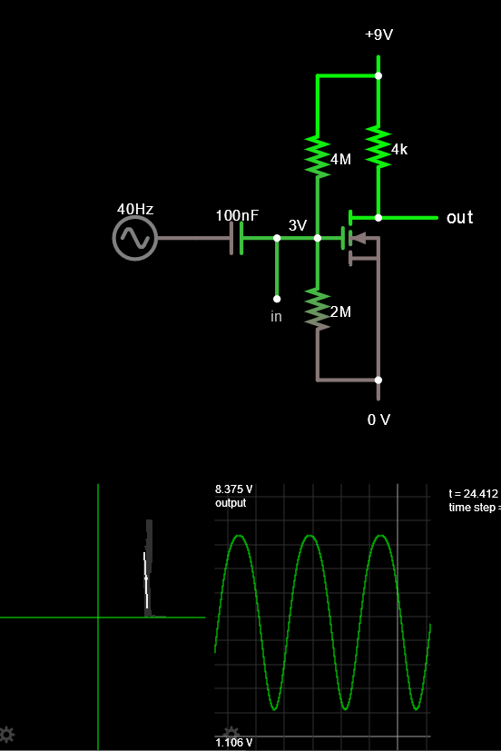
Here is a simulation of a common source amp, showing the in vs. out XY mode (aka Transfer function) and output(t) traces for a FET with a threshold voltage Vt = 2.8 and gain = 20mA/V

enter image description here

\$\endgroup\$
9
  • \$\begingroup\$ I had fun with your simulation... but I can't get rid of the feeling of being too detailed... What does the left graphic represent - maybe a transfer characteristic? I would make the voltage divider with a potentiometer... \$\endgroup\$ Commented May 6, 2020 at 13:45
  • \$\begingroup\$ This simulator becomes so fast to use with practise that you can add so much much detail you get to see the big picture of all points at the same time and then vary any parameter with a a pot slider like FET THRESHOLD Vgs on the right. Here I made the Pullup R a variable like a Pot. YOu can also use real Pot but this is much easier to create as you can define the slider limits for improved sensitivity from range reduction. tinyurl.com/yb9glbq2 \$\endgroup\$
    – D.A.S.
    Commented May 6, 2020 at 14:09
  • \$\begingroup\$ The only missing part is a trigger to this sliding trace, but the time sampling rate can be used under options> time or on each trace for scale \$\endgroup\$
    – D.A.S.
    Commented May 6, 2020 at 14:15
  • \$\begingroup\$ The left was created by a sequence of Add a plot (later to be Y) , , Add next plot (to be X) , Combine , Choose propertiy X/Y , to get the XY transfer function of combined 2 plots. Now without scales. But can be maximized (autoscale) with trace phosphor memory effects. The reason this feels too detailed is because Plots automatically displays the Vmax and Vmin if those boxes are selected in properties of the trace. Or would can choose Power (watt) etc. \$\endgroup\$
    – D.A.S.
    Commented May 6, 2020 at 14:16
  • \$\begingroup\$ The time scale ends up being in "slow motion" as the display of 2k points at some ps, ns, us or ms per sample, unless you choose say 500us per sample or more and slide the simulation speed slider more than 50%. \$\endgroup\$
    – D.A.S.
    Commented May 6, 2020 at 14:18
2
\$\begingroup\$

I will try to answer this very interesting question with simple words...

"Biasing" actually means to add another but reference input quantity to the varying input quantity. If both input quantities are voltages, we can sum them directly by connecting the voltage sources in series. Since the input source is usually grounded, the bias source should be floating. Another but less commonly used way is first to convert the voltages to currents and then sum the currents by connecting the current sources in parallel. Let's consider how the first bias technique is implemented...

1. "Lifting" the base. In AC amplifiers, the bias voltage sources can be implemented by a (floating) charged capacitor connected in series between the (grounded) input voltage source and (grounded) amplifier input. Thus the adjacent amplifying stages are connected by these capacitors; hence the name "coupling capacitors". The advantage of this biasing arrangement is that coupling capacitors can act as floating voltage "sources"... and so we can connect as many such floating sources as we want...

2. "Lowering" the emitter. In DC (ICs) amplifiers, we cannot use capacitors for obvious reasons; so we have to replace them by conventional voltage sources... but they cannot be floating. In this arrangement, the floating amplifier input is connected in series between the grounded input voltage source and grounded bias voltage source. Figuratively speaking, while above we "lifted" the base above the ground, here we "lower" it below the ground. This means to insert a negative bias voltage source between the emitter and ground.

3. "Moving" the base-emitter junction. In contrast to simple transistor amplifying stages with single-ended input where the base-emitter junction is "immovable" (firmly connected to ground), in the more sophisticated transistor differential pair (aka long-tailed or emitter-coupled pair) it "moves" with the variations of the common-mode voltages. So it cannot be biased by a voltage source; it can be biased by a current source from the side of the emitter. Let's consider the MOSFET version of this structure - Fig. 1.
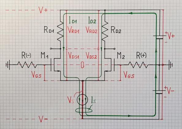
MOSFET differential pair

Fig. 1. MOSFET differential pair

Structure. It consists of two voltage (source) followers which outputs are joined. To bias both transistors (from the side of the sources), the common point is connected through a common element to a negative power supply. This element has the property to keep the current through itself constant. That is why it is named "current source" although it is not a source. It can be thought as of a "current-stabilizing dynamic resistor" that is usually implemented by another MOSFET with constant gate voltage.

VIN = 0. To investigate how the transistors are biased, the input voltage sources are excluded. The gates are simply grounded through resistors R(-) and R(+) so that the bias "current source" can drive the transistors from the side of sources. It makes them adjust their gate-source voltages until the total current through transistors becomes equal to the desired bias current.

VIN = var. Then the input voltages can be applied to gates... and can be varied simultaneously (common mode). The common source point will "move" but the bias current will stay constant.


EDIT: It is interesting to consider the more sophisticated version of this conceptual circuit diagram given in Tako's answer:
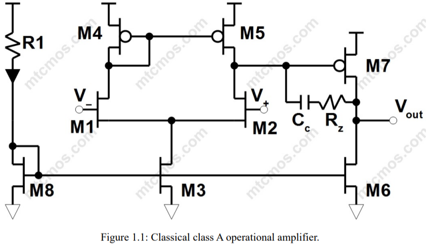
MOSFET differential pair (https://payhip.com/b/5Srt)

Fig. 2. More sophisticated MOSFET differential pair (https://payhip.com/b/5Srt)

The current stabilizing element in the joined sources is implemented by M3 acting as an output current-sinking part of the M8-M3 current mirror; M8 is the input current-setting part of this current mirror (and of the current mirror M8-M6).

M4 and M5 serve as the drain resistors RD1 and RD2. They form another but sourcing current mirror. But what is its function? The idea here is to make a dynamic load pair by M1 and M2 (like M6 and M7 in the output stage). But since it is impossible, they cloned M1 by M5 and made the desired pair by M2 and M5. Fantastic idea, right?

Thus there are two cascaded amplifying stages with dynamic load... and the total gain is huge. Figuratively speaking, the pairs M5-M2 and M7-M6 act as two super-sensitive scales that can hardly be balanced. It can be done only by applying a negative feedback.


It would be interesting to see these ideas in an older BJT implementation:
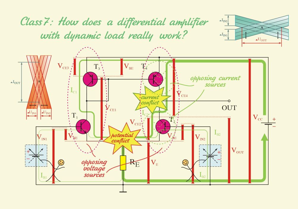
BJT differential pair with dynamic load

Fig. 3. BJT differential pair with dynamic load (visualized)

\$\endgroup\$
2
\$\begingroup\$

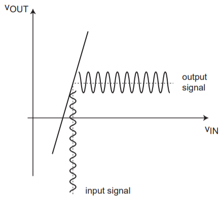
When I started learning CMOS analog IC design I had many similar questions. Your circuit is from Razavi. It is rather to explain amplification properties of CMOS transistors:

enter image description here

Above picture is from: https://ocw.mit.edu/courses/electrical-engineering-and-computer-science/6-012-microelectronic-devices-and-circuits-fall-2005/lecture-notes/lecture19annotat.pdf

Please read it. You have a lot explained there.

In your picture the input signal Vin is on the gate while the output signal is created on the Rd resistor. Depending what is your Vin DC voltage and Vin AC voltage you will get different Vout output signal.

In my opinion, the best thing you can do is not to stop for a long time on such things and go ahead and read and learn more. I recommend you Baker or Camenzind. The more circuits you meet, the more you understand and learn. Then it starts to be simple and obvious. For example take a look on the full circuit:

enter image description here Source: https://payhip.com/b/5Srt ("Preview" button in right top corner)

M3 and M6 transistors are biased by M8 transistor (current mirrors). Your case is similar to M7 transistor, which instead the resistor Rd has M6 transistor on its output. M6 works as a current source so it is seen as a big resistor. The DC voltage on M7 gate is set by M4-M5 current mirror. Then only AC signal is generated when V- and V+ signals start to be different.

\$\endgroup\$
2
  • 1
    \$\begingroup\$ Don't you think we should explain circuits to new contributors in more detail and carefully? Put yourself in their shoes and imagine what they imagine from their point of view when reading our explanations. I tried to do it when enlarging your explanations... \$\endgroup\$ Commented May 6, 2020 at 13:27
  • 1
    \$\begingroup\$ Sure. Good point :). I always try my best. Yesterday, I could not find a good picture for the amplification process for a transistor. Today, I found a better one. Please @Circuitfantasist, add comments or improve the answer if you know what should be done better. Great job with your answer, I added +1. Good point with the feedback. :) \$\endgroup\$
    – Tako
    Commented May 7, 2020 at 8:23
0
\$\begingroup\$

First of all biasing a transistor in ICs isn't much different as in discrete circuits secondly, you can set the R with current source but there are other ways do to so as well. At the end it worth mentioning that coupling capacitors are not used in ICs because it needs a big capacitor and it is not area efficient, so in cases like that you need to calculate it with considering its effect or cancel its effects with inductors

\$\endgroup\$

Your Answer

By clicking “Post Your Answer”, you agree to our terms of service and acknowledge you have read our privacy policy.

Not the answer you're looking for? Browse other questions tagged or ask your own question.