5
\$\begingroup\$

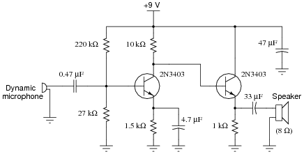
I'm trying to understand the below circuit:

Question #5

I have to analyze an amplifier circuit from a microphone to a speaker and don't understand how it works. I know that the first stage is a voltage divider, but I can't figure out what the second stage is or how it works? In which stage does the amplification take place? I would really appreciate any help!

\$\endgroup\$
2
  • 6
    \$\begingroup\$ It sounds like you've gotten a bit ahead of yourself. How much do you understand about how a transistor works? We're going to need to know where you're at in order to come up with an answer that will be useful to you. \$\endgroup\$
    – Dave Tweed
    Commented Nov 26, 2012 at 13:15
  • \$\begingroup\$ i am very new to transistors and really understand basic circuits only \$\endgroup\$ Commented Nov 26, 2012 at 14:18

7 Answers 7

27
\$\begingroup\$

Let's put some part reference designators on your diagram.

Annotated

Always number all the parts. Then it is easy to discuss the diagram. Instead of "the emitter resistor of the second transistor" we just say R5.

  • C1: This is a coupling capacitor which allows the AC signal to pass but blocks DC. It protects the microphone's coil from receiving a DC current from the amplifier's bias circuit and protects the amplifier's bias circuit from being disturbed by the impedance of the microphone. C1 transmits the voltage fluctuations from the microphone, superimposing them upon the bias voltage between R1 and R2.

  • R1 and R2: These resistors form a voltage divider, establishing a voltage-divider bias for the base of transistor Q1. From a 9V power supply, R2 will develop about 1V. That's enough to forward bias the base junction of Q1, turning the transistor on.

  • Q1: This BJT is the heart of the first amplification stage, a common-emitter (CE) voltage amplifier. Its job is to transform variations in the base current caused by the microphone voltage variations arriving over C1 into current variations through the collector-emitter circuit R3, R4 and C2.

  • R3: This is the load resistor for the CE voltage amplification stage. Variations in current controlled by Q1 cause R3 to develop a voltage. This voltage is the output of the Q1 stage, directly conveyed to the base of Q2. The voltage is inverted with respect to the microphone signal. When the signal swings positive, more current flows through R3, developing a greater voltage drop. The top of R3 is pinned to the 9V power rail, so more voltage drop means that the bottom of R3 swings more negative.

  • R4: This emitter resistor provides feedback to stabilize the DC bias of Q1. The bias provided by R1 and R2 turns on Q1 using a voltage of about 1V, mentioned above. This causes current to flow through the transistor. This current causes a voltage in R4. The transistor "rides" on this voltage. So the voltage opposes the 1V of bias. According to some rule of thumb calculations, R4 will develop about 0.3V, which is the voltage that is left over when we take the 1V bias voltage between R1 and R2, and subtract the base-emitter voltage drop of 0.7V. This 0.3V over 1500 ohms means that about 0.2 mA of collector current will flow through the transistor, at quiescence. This bias current also flows through the 10K R3 resistor, where it gives rise to a voltage of 2V. So the output of Q1 is biased approximately 2V below the 9V power rail.

  • C2: This capacitor bypasses the R4 resistor for AC signals. The R4 resistor has the effect of feedback. The amplified current passes through R4 and develops a voltage, and Q1 rides on top of this voltage. The voltage being amplified is the difference between the input and the emitter. So R4 provides negative feedback, which reduces gain. By introducing C2, we get rid of this feedback for AC signals. AC signals do not experience negative feedback, and so the gain is much higher for those signals. R3 and R4 provide a stable DC bias for Q1, and C2 "cheats" around it, creating a higher gain for AC, so that the amplifier has a wider swing around the bias point (which, recall, is about 2V below the power rail). A lot of voltage gain is needed because microphones put out a rather small signal, and all the amplification is being done by a single stage.

  • Q2: This transistor is set up as a current amplifying emitter-follower stage. Note that there is no load resistor similar to R3 in the previous stage. Instead, the output is taken from the top of the emitter resistor R5.

  • R5: What happens here is that the top of resistor R5 follows the voltage applied to the base of Q2. It is simply that voltage, minus 0.7V. As the voltage at the base swings, the voltage at the top of resistor R5 goes through the same swing. This voltage is applied to the speaker through C3.

  • C3: Another blocking capacitor. It prevents DC from flowing into the speaker, which would damage the speaker and also cause a lot more bias current to flow through Q2, since the speaker's impedance is a lot lower than that of R5.

  • C2: This is a power-supply decoupling capacitor. In several places in the circuit, AC signals return to the power supply either through the 9V rail or through the common return (ground). These currents can develop a voltage across the internal impedance of the power supply. C2 provides a short circuit for these AC signals. Without power supply decoupling, current variations in Q2 could feed back into the Q1 stage, giving rise to oscillations. C2 also helps to keep stray noise from the power supply, such as power supply ripple, from affecting the circuit. Another way to look at it is that the capacitor provides current in response to sudden demands by Q2.

The Q2 stage is needed because, even though it does not amplify voltage, it amplifies power. It does that because it is able to deliver more current than Q1. Q1 has load resistor R3, which gives it a rather high output impedance. If the speaker were connected to the Q1 stage output, hardly any sound would come out of it because the Q1 stage cannot maintain its voltage into just an 8 ohm load. Q2 has no collector resistor, and so the output impedance is low. Current flucutations flow freely from the power supply, through the transistor's collector and across C3 to the speaker.

The Q1 stage is needed because a current driving stage like the one built around Q2 doesn't have any voltage gain. The Q2 stage alone could take the voltage from the microphone and put it across the speaker. Now it would be better than connecting the microphone directly to the speaker, because the microphone would be isolated from driving the low impedance of the speaker. But, in spite of that, would simply not be loud enough. Getting a reasonably loud sound out of the speaker requires a much higher voltage level.

The jobs of amplifying voltage, and then amplifying the current which enables that voltage to be put across a low-impedance load such as a speaker, are best implemented separately.

\$\endgroup\$
1
  • \$\begingroup\$ Just a quick pedantic note about R5, C3 and the speaker. For signals, the emitter "sees" the parallel combination of R5 and the speaker impedance (assuming the impedance of the coupling C3 is negligible for signals). Since the speaker impedance is relatively small, from a signal perspective, R5 is effectively "not there". In other words, R5, like R4, is effectively bypassed for signals. From an AC analysis perspective, Q1's emitter sees ground and Q2's emitter sees slightly less than 8 ohms. So, it's not quite correct to say that the output voltage is applied to the speaker through C3. \$\endgroup\$ Commented Nov 27, 2012 at 0:34
2
\$\begingroup\$

The BJT transistor is a current amplifier when the base emitter voltage is 0.6~0.7V like a diode drop. The collector-base is also a diode but is only lightly doped and reverse biased to function as a bas current controlled current amplifier. We use imepdance to convert current to voltage gain in the 1st stage and the second stage is need to amplify current to drive higher power (low resistive) loads.

The 1st stage we call "H biased" as it resembles the schematic, where the 2 input base reistor ratio sets the base then the emitter voltage is 0.65V lower and thus the emitter DC current can be predicted from hFE.

From from the collector /emitter ratio there is more drop on the collector so for the same current, there is now a voltage gain for DC as well as AC. BUT since the Emitter capacitor provides a much lower "impedance: This ratio for AC is much higher and is limited by the internal emitter reistance (not shown in schematic). We can estimate the voltage gain by looking at the specs and estimate the internal resistance for Re. This works well for small input signals less than 10% of the Vbe drop, since for AC the emitter cap does not allow much voltage swing. 100mV max is already distorted quite a bit. So we are converting voltage to current with impedance (V=I*R) and thus using the collector output amplifying voltage with impedance ratio and current gain of the transistor.

In the 2nd stage it is pure current gain and the ac voltage on the emitter matches the base as long as the Vbe stays at 0.6~0.7Vdc. Putting too much ( too low value) of a load like 8 ohms wont work on a 1Kohm emitter bias and will fail.

Why? Because the transistor actually controls the current by pullup to the supply. The resistor must pull down in order for the amplifier to be bi-directional for AC signals. With no emitter resistor to ground the emitter voltage would just float at the maximum AC voltage like a poitive peak detector.

Thus common speaker amplifiers use complementary pair output schemes with PNP and NPN devices.

This simulator allows to change any value and probe voltage, current & power.

Since the collector resistance is about the same as the input reistance, we say it is more a voltage amplfier, whereas the 2nd stage with emitter output is a current amplifier with < unity voltage gain. The ac load must not be < than the DC resistor.

Side comment: putting 2 complementary (in series) emitter followers ( NPN, PNP for + PNP then NPN for -ve) with large resistors and big capacitors makes a zero offset AC peak detector.

\$\endgroup\$
1
\$\begingroup\$

My broad and beginner answer: The first stage is a "class A" amplifier that provide some voltage gain. This gain is proportional to the transistor beta. The second stage is an emitter follower and it is basically just boosting the current: it's voltage gain is about 1, but it allow you to drive the load of the speaker without affecting the first stage. The emitter follower also known as common collector, has a large output impedence about \$\beta * R_{load}\$ and a low output impedence of about \$R_{load}\$ in parallel with \$R_{input}/\beta\$.

\$\endgroup\$
4
  • \$\begingroup\$ i still dont really understand the second stage, why is it necessary? \$\endgroup\$ Commented Nov 26, 2012 at 14:45
  • 1
    \$\begingroup\$ because you can't connect the 8 Ohm load directly to the first stage since it is not a "power" stage, but it just provide the voltage gain. \$\endgroup\$ Commented Nov 26, 2012 at 14:49
  • \$\begingroup\$ You cant connect an AC coupled load lower than the DC Re value either. \$\endgroup\$
    – D.A.S.
    Commented Nov 26, 2012 at 15:21
  • \$\begingroup\$ @FlorianOtt, the output impedance of the first stage is roughly 10k ohms. If you connect the speaker (with series capacitor) directly to the output of the first stage, over 99% of the voltage gain is lost due to voltage division. The second stage presents a relatively high impedance to the first stage and has a relatively low output impedance. Such a stage is commonly called a "buffer amplifier": en.wikipedia.org/wiki/Buffer_amplifier#Voltage_buffer \$\endgroup\$ Commented Nov 26, 2012 at 16:27
0
\$\begingroup\$

"Stage" in an amplifier means "active device (here, a transistor) together with all its support circuitry". So this is a 2 stage amplifier. Given that, have another go...

\$\endgroup\$
0
\$\begingroup\$

The output of the microphone is a very small variance in voltage. The voltage divider biases this upwards so it's centered around 0.9V. That's enough to turn on the first transistor into its "linear" region, where the current flowing vertically (through the 10k resistor) is a multiple of the current flowing in through the base. That produces an inverted, amplified signal. The other transistor amplifies it futher.

("have to analyse" - is this a homework question?)

\$\endgroup\$
3
  • 2
    \$\begingroup\$ No, the second stage does not invert. \$\endgroup\$ Commented Nov 26, 2012 at 14:25
  • 1
    \$\begingroup\$ so if only the first stage inverts is the output inverted? does this have any effect on the audio? \$\endgroup\$ Commented Nov 26, 2012 at 15:12
  • \$\begingroup\$ Removed erroneous inversion. \$\endgroup\$
    – pjc50
    Commented Nov 26, 2012 at 15:20
0
\$\begingroup\$

but I can't figure out what the second stage is or how it works? In which stage does the amplification take place?

Sure you can figure it out, you just need a little help.

If you recall that the base-emitter voltage of a transistor operating in the active region is nearly constant, then you can figure out that the 2nd transistor cannot be a voltage amplifier; the signal voltage on the emitter is almost the same as the signal voltage on the base.

So, the voltage amplification must be due to the 1st transistor circuit. This transistor is configured as a classic common emitter amplifier.

The reason for the 2nd transistor circuit may not be immediately obvious but it is, in fact, crucial to the proper operation of this amplifier.

The speaker is a very low impedance load. For significant voltage gain, the collector of the 1st transistor must be connected to relatively high impedance as the gain is proportional to this impedance.

If you connect the speaker (through the coupling capacitor) directly to the collector of the 1st transistor, the speaker's impedance is in parallel with the collector resistor so the collector is now connected to a very low impedance and thus, the voltage gain falls to nearly zero.

However, the 2nd transistor is configured as a common collector amplifier which acts as a voltage buffer. Essentially, looking into the base of the 2nd transistor, the 8 ohm speaker impedance is multiplied by the beta (plus 1) of the 2nd transistor.

If the beta is 100, the speaker impedance "looks" 101 times larger through the base so, by connecting the base of the 2nd transistor to the collector of the 1st transistor, some voltage gain is still possible from the 1st stage.

\$\endgroup\$
3
  • \$\begingroup\$ Kinda late to the party but it looks like the input impedence to the speaker will be some 800 ohms , so won't most of the voltage sit on the 10k resistor ? Looks to me like this isn't going to amplify anything . \$\endgroup\$
    – Vrisk
    Commented Aug 1, 2017 at 16:00
  • \$\begingroup\$ @Vrisk, no, you're not thinking about it correctly. From an AC small-signal perspective, the 10k collector resistor is (essentially) in parallel with the 800 ohms rather than in series so no voltage division. \$\endgroup\$ Commented Aug 2, 2017 at 1:26
  • \$\begingroup\$ Ah I see , but what about the 1k resistor on the output transistor , I don't think the output capacitor will be able to push much current through it ( .5 amps through 1k resistor for 4 volts on negative half cycle ?) \$\endgroup\$
    – Vrisk
    Commented Aug 3, 2017 at 14:52
0
\$\begingroup\$

The highest voted answer here is sufficient but I want to add a comment that the output resistor (R5) which is also known as "Re" for the "emitter resistor" in your voltage follower circuit is too large.

This is the problem with Class A amplifiers (the emitter follower you have) is that the output current will be equal to the bias current. Basically since your load is AC coupled with the output capacitor, and your load is 8 ohms, R5 will also need to be 8 ohms, otherwise the transistor won't be able to give you enough negative swing to be symmetrical.

Changing R5 to 8 ohms will dissipate a lot of power. So if you're DC biased at 6V (6/8ohms = 0.75) so the power is 4.5Watts... so that resistor will get very hot. The other option is to not AC couple the load, but most speakers can't handle DC current so this is not really an option. I just wanted to mention this because this is a common problem with Class A amp tutorials and schematics on the internet - it won't work if you simulate it in LT spice because Re needs to match the load.

\$\endgroup\$

Not the answer you're looking for? Browse other questions tagged or ask your own question.