The current in PMOS flows from the Source to the Drain terminal, and that can only happen if the Gate terminal is set to Low. Silly question, but why is that so?
To answer this question you have to know the working principles of the Mosfet transistor. Generally a PMOS can be turned on if \$ V_{G} \$ < \$ V_{S} \$ and that is because when that kind of voltage is applied to the gate of the PMOS, the electrons present under the oxide layer are pushed downward into the substrate with a repulsive force which leaves us a depletion region populated by donor atoms and just under the oxide we will have a layer of Holes (Which are the charge carriers for PMOS). Then again i strongly suggest that you read these principles yourself.
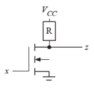
how can we use this to get the NOT logic gate (As shown in the second
image)?
The image that you have provided is a NOT logic gate using NMOS. I'm not sure what you are asking here but if you want to know how it works, it's simple, when the Gate is low, the NMOS is turned OFF, therefore no current flows from Drain to Source so there will be no Voltage across the resistor and output will be equal to VCC(HIGH). If the Gate is high, the NMOS is turned ON and current flows through the NMOS therefore output is connected directly to the ground so the output becomes LOW.
This is the same NOT gate using a PMOS:

simulate this circuit – Schematic created using CircuitLab
Please try and analyze this circuit for yourself.


