0
\$\begingroup\$

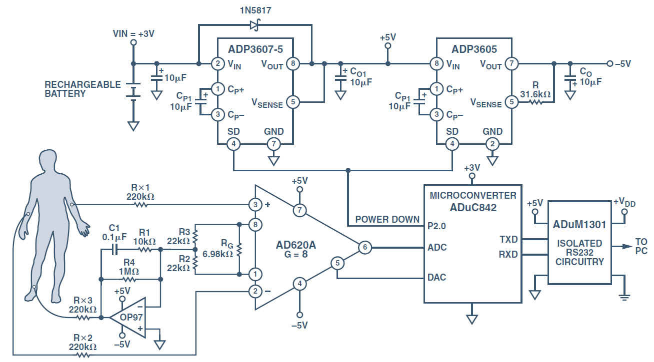
I am trying to implement the below circuit (from) without ADuC842, I will use Arduino mega2560 ADC.

enter image description here

the circuit generates -5V to 5V rail to rail voltages for ad620a and they control ref voltage via DAC to adjust offset dynamically.

from the link, To avoid output saturation, the usable gain is limited by the output swing and the maximum input voltage to the IA. With a +-5 V power supply, the output swing of the AD620 is about +-3.8 V; and the maximum input is +-5 mV plus a variable normal-mode dc offset of up to +-300 mV, allowing a maximum gain of 12.45. Here, the gain is conservatively set to 8 (+-1%), using RG = 8.45 kOhm.

I need to change how Ref pin voltage is supplied,

I have the following doubts?

if the voltage at ref pin is 5V the out swing between 0-5?

how can I get the output of ad620 to swing between 0-5V (pin 6 ad620) what voltage should I apply to ref pin

dummy doubts

is it possible to measure the negative voltage from the microcontroller ADC?

can aduc842 generate a negative voltage from DAC?

\$\endgroup\$
2
  • \$\begingroup\$ Vref is a dynamically adjustable voltage that is produced by the DAC to try and make the voltage swing centred around the mid point of the ADC's analogue input range. Why would you want to change this sensible arrangement? Replacing with a fixed voltage (as per your title) is missing the point I feel. Might you be trying to solve a problem that might be solved in a better way (XY)? \$\endgroup\$
    – Andy aka
    Commented May 29, 2020 at 9:45
  • \$\begingroup\$ I need to use Arduino mega2560 for this one, is there any other issue? if i change the MCU used in above schematic \$\endgroup\$
    – komto909
    Commented May 29, 2020 at 9:57

1 Answer 1

1
\$\begingroup\$

Is it possible to replace the ref pin of AD620A with a fixed voltage?

Probably not is the simple answer.

The DAC output (under software control) will examine the ADC digital output and make an estimate of whether the signal it is receiving needs slightly lowering or slightly raising in its DC offset level. It does this to avoid signal clipping. Clipping the signal means that the top or bottom section of the signal is "out of range" and causing the ADC to end-stop.

This needs to be avoided to achieve maximum dynamic range and so, the DAC will constantly tweak the offset to centralize the signal fed to the ADC.

If your proposed MCU doesn't have a DAC output, you should be able to make an effective DAC output using PWM and a low pass filter. This can then be used to feed pin 6 of the AD620.

\$\endgroup\$
2
  • \$\begingroup\$ if accidentally negative voltage appears on the output of the ad620 can it damage the ADC input of MCU? \$\endgroup\$
    – komto909
    Commented May 29, 2020 at 10:35
  • 1
    \$\begingroup\$ It's a good point and I would definitely place a 10 kohm resistor in series with the ADC input. This will limit the current to acceptable levels should the output from the AD620 go negative (or highly positive). \$\endgroup\$
    – Andy aka
    Commented May 29, 2020 at 10:40

Your Answer

By clicking “Post Your Answer”, you agree to our terms of service and acknowledge you have read our privacy policy.

Not the answer you're looking for? Browse other questions tagged or ask your own question.