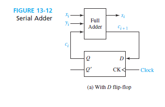
The first figure (from Fundamentals of Logic Design, Roth/Kinney, 6th Ed, p.404) shows a serial adder which feeds in operand bits and stores the sum, and uses a D flip-flop to store the carry-out from each bit pair and load it back in as the next carry-in.
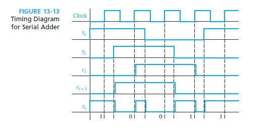
The second figure (from Fundamentals of Logic Design, Roth/Kinney, 6th Ed, p.405) shows a timing diagram for this same serial adder.
My question is: is there a good reason why the delay in loading the operand bits (x_i and y_i) would be depicted as being longer than the delay in loading the carry-in (c_i)? This seems important, because (as shown in the timing diagram) it leads to glitches in the sum, s_i.
I have assumed (though the textbook does not absolutely confirm this) that shift registers made of D-type flip-flops (like the one for the carries) would be used to feed in the operand bits and store the sum. If so, surely the delay for loading x_i and y_i would be identical to the delay for loading c_i?
If not, can anyone cast light on another reason why the timing diagram depicts things this way? I have searched unsuccessfully online for an answer, and one is not contained in the textbook itself to my knowledge.
To be clear: my suspicion is that the authors made a mistake (I am guessing they did not allow for flip-flop propagation delay in loading c_i) -- but I'd like to get a knee-jerk response from more experienced folks indicating whether they would tend to agree with me, or whether I'm missing something really obvious? Thanks!


