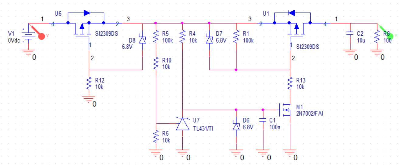
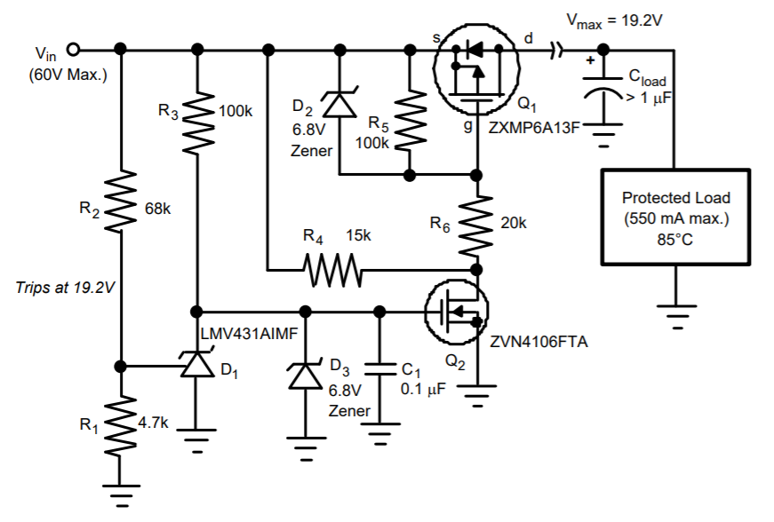
Currently I'm working on a project that will be implemented in a 12V automotive electrical system. To protect the onboard DC/DC, I decided to add reverse polarity protection as well as load dump protection to the 12V+ input. After some research (and referencing this application note), I designed the following circuit (note: some component values were changed for BOM optimization):
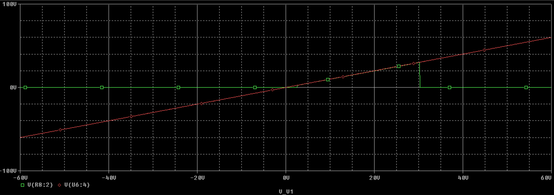
 Which produces the following simulation result (reverse polarity and over voltage (>30V) cutoff), as intended:
 My main question is that in the TI AN they include an additional resistor from the drain of the n channel mosfet to the source of the p channel overvoltage mosfet (R4 in the below schematic).
 What is the function of this resistor? The AN mentions its to bias Q2 and satisfy its drain leakage in the off state. Wouldn't R5 + R6 complete this function anyway?
-
\$\begingroup\$ Welcome. The sum of R5 and R6 is much greater than the value of R4. \$\endgroup\$– user105652Commented Jun 29, 2020 at 0:46
-
\$\begingroup\$ What about TVS? I think it is custom(?) to place it directly after the polarity protection, so I suppose directly after D8 in your schematic. It should roughly be at 18V and you probably need the automotive spec >1500W ones. \$\endgroup\$– LundinCommented Jun 29, 2020 at 8:50
-
\$\begingroup\$ Is it more commonplace to use an automotive TVS in this application? I'm aware of the high power units designed for load dump transients but I wasn't sure if they were the more desirable solution in this case. \$\endgroup\$– mkeCommented Jun 29, 2020 at 14:26
-
\$\begingroup\$ Can you tell me which simulator you used? \$\endgroup\$– Eduardo CardosoCommented Feb 18, 2021 at 19:10
3 Answers
@jp314 has already answered exaustively to the second part of your question, thus I'll focust on the first part: and metodologically, I'll refer preferably to your schematics components labels, and only when in need I'll use the ones shown in the excerpt of the TI AN.
What is the function of this resistor?
Looking at the ZVN4106FTA datasheet (p. 3 of 6) you see that the \$I_{DSS}\$ can be as large as \$50\mu\mathrm{A}\$: this large leakage current implies that, whitout the \$R_4\$ resistor and when \$M_1\$ is OFF , you can have a gate-to-source voltage as high as $$ V_{GS}\simeq -V_{R_1}=-R_1I_{DSS}\simeq -5\mathrm{V}. $$ Having a look to the ZXMP6A13F datasheet (p. 4 of 8), you see that this voltage goes well beyond the maximum thresold voltage \$V_{GS_\mathrm{(th)}}\$ of the MOSFET (\$V_{GS_\mathrm{(th)_\max}}=-3V\$ as stated in the datasheet). Therefore, given the values of \$R_1\$ and \$R_{13}\$, the use of a pull-up resistor like \$R_4\$ connected on the drain of \$M_1\$ is absolutely needed since, apart from favourable statistical combinations (which may happen and usually do happen when you build your first prototype of the circuit ;) ) otherwise you may find that the \$U_1\$ MOSFET never goes OFF.
Finally, just for the sake of completesness:
The AN mentions its to bias Q2 and satisfy its drain leakage in the off state. Wouldn't R5 + R6 complete this function anyway?
Yes, you can choose \$R_5\$ and \$R_6\$ of suitably lower values, in order to obtain the same voltage division while avoiding excessive leakage dependent biases. For other problems related in doing so, see the answer of @jp314.
Yes, (their) R5 & R6 can perform that function, but not as well, depending on your constraints.
To ensure the 2nd FET turns on well at low VBATT, you need to ensure that your R1 >> your R13; this ensures that at low VBATT, most of the supply voltage (VBATT*R1/(R1+R13)) appears across the VGS, turning the device on. However you can't make R13 too low, or at higher battery voltages, you will have too much current in the zener (Zener current = (VBATT-6.8)/R13) which could overheat it. You can't make R1 too high, or the turn off time will become too large.
Adding their R4 provides good turn-off time (approx. proportional to 1/(R4+R6)), but doesn't overpower the zener.
In fact, you could use R4 and eliminate R5 with no noticeable effect.
Be careful because not only are load dumps possible (and are relatively slow -- < 1 ms rise time), but other sharp high voltage transients can occur (e.g. double battery jump start @ 26.5 V, impulse noise). C1 also slows down the turn-off of the circuit at high input voltages (approx t= C.V/i = 100n*6.8/15mA = 40 us); 10 nF would be safer.
Check LTC4364 from Linear (now analog). It provides input voltage limiting, under-voltage and over-voltage protection, current limiting and over-current trip with delay depending on degree of overloading with recovery to your choice - automatic with cooling down delay or latched off (manual recovery or by re-application of power). It also provides two flags - one indicating protective intervention, the other controlling eventual downstream DC/DC converter. The chip requires external n channel MOSFET (or one more for reverse current protection if needed).
