It is hard to fit everything in my title so please read ahead to understand the whole thing. I am trying to design a circuit that can meet a few requirements but having a lot of trouble trying to make it work.
The design uses a SPDT switch to either power on or off a device.
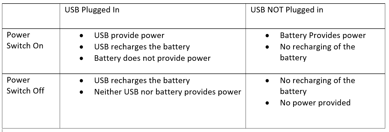
When the SPDT switch is turned on, the device will be powered from either a 3.7V LiPo battery or USB power depending on whether the USB-C port is plugged in or not.
When the USB-C port is plugged in and providing the 5V, the battery will be recharging from it regardless whether the SPDT switch is on or off. The battery will also stop providing power to the device when the USB is plugged in and the device is turned on.
If there is NO USB-C plugged in and the SPDT is turned on, the battery power will provide the nominal 3.7V to a 5V boost IC before providing the power to the device. But the battery cannot provide current flowing back into the recharge circuit (i.e. prevent the battery from trying to recharge itself).
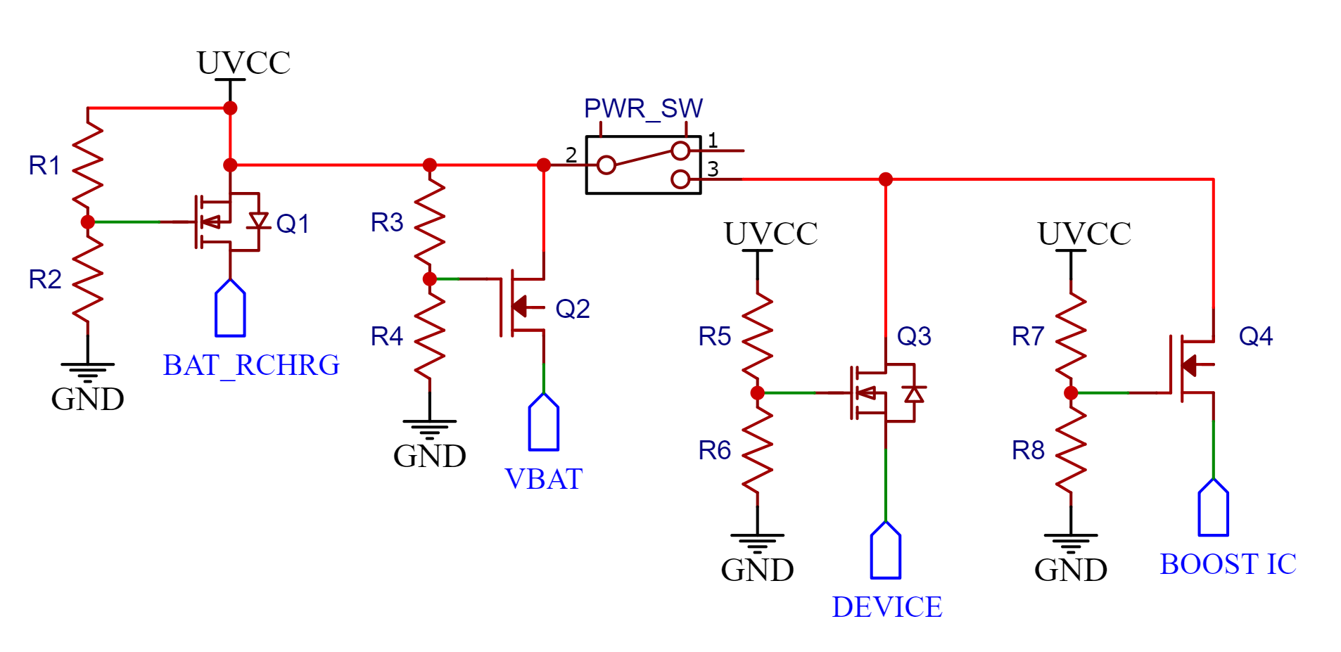
I thought of one way that might work using a combination of enhancement and depletion N-channel MOSFET. A picture of it is attached below.
Here is my logic behind it. UVCC is the VBUS line from the USB port.
If the UVCC line is 5V (when the USB is plugged in), there is enough voltage from the divider (R1 & R2) to turn on Q1, allowing the USB 5V to connect to the LiPo battery recharge/protection circuit. It will also turn off Q2, cutting off the 3.7V nominal voltage from the battery to the UVCC line. Q3 will turn on and Q4 will turn off. Thus, allowing UVCC (5V) to go directly to the device when the power switch is on.
When the USB is NOT plugged in (UVCC < 4.2V), Q2 will be turned on and allow the LiPo Battery to provide current. Q1 will be off to prevent the battery from trying to recharge itself. Q3 and Q4 will be off and on, respectively. Thus, the battery current will flow into the 5V boost IC before going to the device.
I’d appreciate any feedback on this design as well as any suggestions of other circuit design that can meet the requirements described above.
Thanks!
EDIT: Here is a truth table to help understand the requirements


{}code formatting button (or four spaces at the start of each line) to force fixed width font. \$\endgroup\$