1
\$\begingroup\$

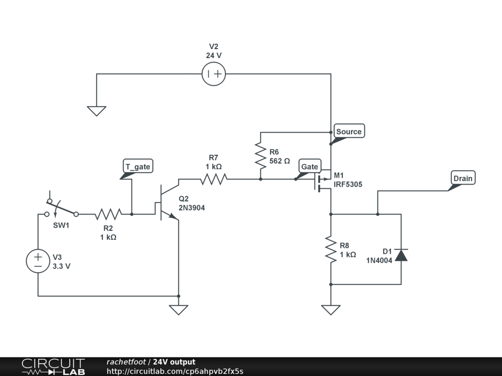
I'm trying to control 24V solenoids using logic level inputs at 5V. The following circuit works when replacing both power loops with a single 9V battery, except that the voltage across the gate and source is not 0 as expected when the switch is closed.

When attached to the actual components with the correct voltages, the MOSFET always powers the drain, regardless of whether the switch is closed.

Can anyone tell me why the circuit works differently than in the simulation? How can I improve it?

enter image description here https://www.circuitlab.com/circuit/p6ahpvb2fx5s/24v-output/

Edit: The load (solenoid) is represented by R8 in this schematic

\$\endgroup\$
1
  • 1
    \$\begingroup\$ where does the solenoid connect in the circuit? \$\endgroup\$
    – jsotola
    Commented Aug 1, 2020 at 22:44

2 Answers 2

1
\$\begingroup\$

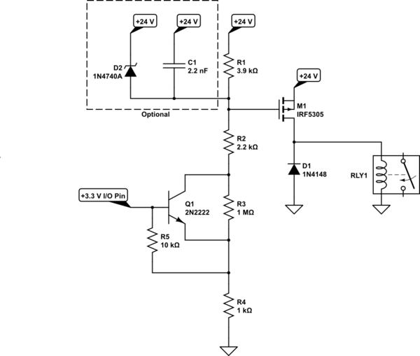
The following schematic is intended to offer the following features:

  • Extremely low drive current required from the I/O pin because the BJT is operated in active mode instead of saturated mode. Therefore the I/O pin voltage (sinking or sourcing in this circuit) should be very close to the MCU rails and the control line will work even with rather feeble drivers.
  • Predictable gate-to-source voltage near the preferred value of \$-10\:\text{V}\$ for optimal operation.
  • Fully resistive paths from gate to both power rails.
  • Diode path for dissipating energy from relay's magnetic field collapse.
  • Optional capacitor to counter the BJT base-to-collector capacitance from exceeding \$-10\:\text{V}\$ gate-to-source voltage when switching off. (PFET has its own capacitance that is probably more than sufficent, though.)
  • Optional zener to protect PFET gate.

schematic

simulate this circuit – Schematic created using CircuitLab

Most relays are specified to operate at 70% of their rated voltage, so I'm not too worried about wrapping the circuit with a large capacitor. I'd probably avoid it unless experience proved otherwise.

Edit

Feel free to use most any diode for the above circuit. Any of the 1n400x will work fine, as well as the 1N4148. A better (but more expensive) circuit might use a zener oriented in the opposite direction as the diode as a way of increasing the coil voltage when its magnetic field is collapsing and thereby shortening the time required.

Also, since the above circuit is operated in active mode you will need to modify \$R_4\$ if you change the MCU rail voltage. In the above circuit, you should want about \$2.6\:\text{mA}\$ in \$R_4\$. So, if you used a \$5\:\text{V}\$ rail, you'd want to change \$R_4\$ to about \$1.5\:\text{k}\Omega\$. (I calculate \$R_4=\frac{V_\text{CC}−700\:\text{mV}}{2.6\:\text{mA}}\approx 1.65\:\text{k}\Omega\$.) That's the only change needed, though it is also possible to make adjustments to \$R_1\$ and \$R_4\$ together, if you prefer.
\$\endgroup\$
3
  • \$\begingroup\$ Very nice, thanks. Would I be able to use the 1N4004 and 2N3904 that I already have for D1 and Q1 instead? \$\endgroup\$
    – boileau
    Commented Aug 2, 2020 at 9:56
  • \$\begingroup\$ By the way, is your schematic sensitive to the I/O voltage? I was considering powering my MCP23017 (I/O expander) with 5V instead. \$\endgroup\$
    – boileau
    Commented Aug 2, 2020 at 10:03
  • 1
    \$\begingroup\$ @boileau Yes, use those devices. Yes, since it is operated in active mode you would need to modify \$R_4\$. You want about \$2.6\:\text{mA}\$ in \$R_4\$. If you used a \$5\:\text{V}\$ rail you'd want to change it to about \$1.5\:\text{k}\Omega\$. (I calculate \$1.65\:\text{k}\Omega\$, to be exact, as \$R_4=\frac{V_\text{CC}-700\:\text{mV}}{2.6\:\text{mA}}\$.) That's the only change needed. \$\endgroup\$
    – jonk
    Commented Aug 2, 2020 at 10:15
2
\$\begingroup\$

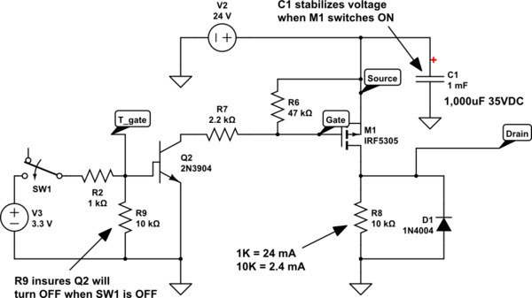
Q2 needs a 10 K pull-down resistor at the base to ground points. Left floating a transistor will not necessarily be 'OFF', so you make make sure transistor base (and gates) never float.

Also, R7 and R6 could be 10 times their value, reducing power consumed by Q2 when it is ON. The MOSFET input impedance is very high, many megohms, so no need to drive it with current. R7 should be less than R6. I would make R7 10 K and R6 47 K.

Diode D1 which is to suppress back EMF from a solenoid or other inductive load could be a faster BA157, but the 1N4xxx series is ok for slow switching speeds.

I copied and improved your schematic. This should work better.

schematic

simulate this circuit – Schematic created using CircuitLab

\$\endgroup\$
2
  • \$\begingroup\$ Thanks. So the main issue was the lack of pull-down resistor at Q2, right? Regarding resistor sizes, I was under the impression that large resistances will cause the MOSFET to switch slower. Although if it's a matter of a few ms, that's not an issue for my purposes. \$\endgroup\$
    – boileau
    Commented Aug 2, 2020 at 9:58
  • \$\begingroup\$ So I added the pull down resistor and reversed R6 and R7 from my original circuit and then discovered that Q2 was placed backwards. With those changes the circuit works as expected. Thanks for the help. \$\endgroup\$
    – boileau
    Commented Aug 2, 2020 at 12:24

Your Answer

By clicking “Post Your Answer”, you agree to our terms of service and acknowledge you have read our privacy policy.

Not the answer you're looking for? Browse other questions tagged or ask your own question.