0
\$\begingroup\$

I've been trying to tame an LM318 opamp in order to replace the LM741 in a circuit because I need to buffer a higher frequency sine wave than the LM741 likes (1Mhz).

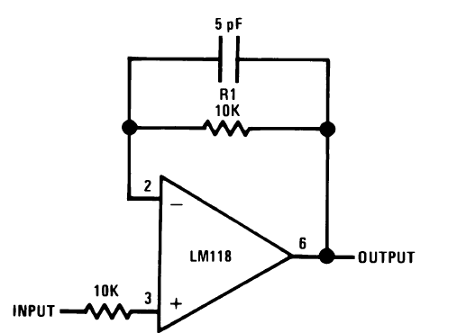
The datasheet shows the following example circuit right on page 1: enter image description here
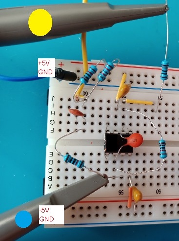
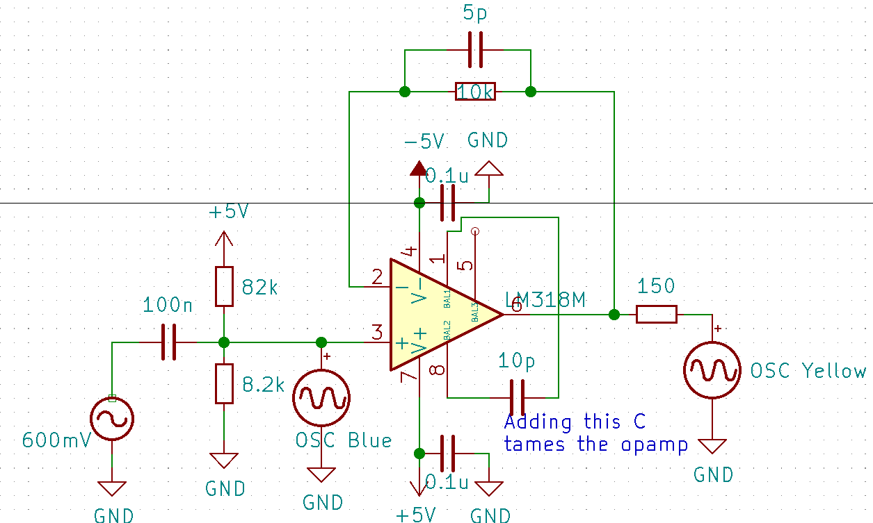
Ok, so I build this up, and am feeding a 200kHz signal at 0.6V peak-to-peak offset to a small, positive value, with a +5 and -5V rail: enter image description here enter image description here
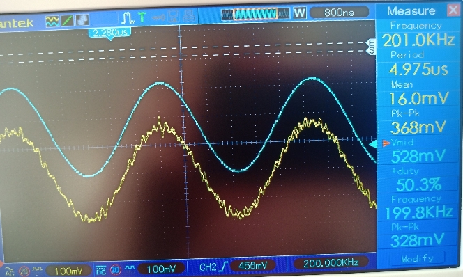
However, instead of buffering the voltage, the amplifier starts to self-oscillate: enter image description here
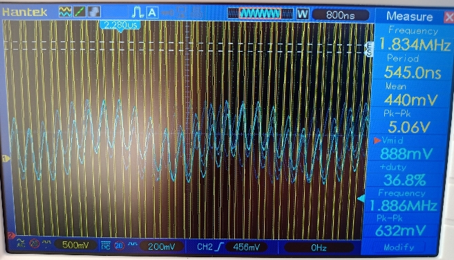
Not what was supposed to happen, so I decided to solder the circuit to perfboard, but much to my disappointment with the same result.

I thought maybe adding a resistor before the oscilloscope at the output would help so as to not drive a largely capacitive load, but that made no measurable difference

After lots of research I came across a post that recommended decoupling pin 1 and 8 of the opamp with a tiny capacitor (I used 5pf, but tried other values, larger didn't have a visible effect), and it seemed to tame the beast a bit, but the output was still distorted. Note that this is not mentioned anywhere in the datasheet. however, in the internal diagram on page 15 there seems to be C3 (28pF) connected across pins 1 & 8 internally, so not sure why a tiny 5pF would make a difference here.

enter image description here

This sure isn't by design, so my question is basically, what am I doing wrong in using this device and how can I fix this?

Is it not suitable for this purpose and I should consider a different chip?

\$\endgroup\$
4
  • \$\begingroup\$ Using a breadboard can cause this kind of problems. Soldering the components to a stripboard could help \$\endgroup\$ Commented Aug 6, 2020 at 17:55
  • \$\begingroup\$ What power supply are you using? Are the rails clean? Have you checked? \$\endgroup\$
    – Andy aka
    Commented Aug 6, 2020 at 18:57
  • \$\begingroup\$ @RohatKılıç I did that, but unfortunately this didn't make a difference. \$\endgroup\$
    – namezero
    Commented Aug 6, 2020 at 19:26
  • \$\begingroup\$ @Andyaka Hello. Yes, the supply rails measure within 10mV of ripple. Given the answer provided, I think I will adjust the values of the feedback capacitors when I make a PCB. \$\endgroup\$
    – namezero
    Commented Aug 6, 2020 at 19:29

3 Answers 3

1
\$\begingroup\$

You are using a solderless breadboard, which is not ideal. There are parasitic capacitances of similar order of magnitude to the 5pF capacitor.

If you increase the 5pF to 10 or 15pF it will probably stabilize it, but of course on a PCB it will behave a bit differently.

You should have the 100nF bypass capacitor directly from pins 4 to 7 (power supply) close to the chip. I don't see where your lower "GND" is connected to the upper one, but the capacitor should be much closer.

So, no don't (necessarily) consider a different chip, in fact a higher performance chip might be worse. Consider a better construction method such as a PCB.

\$\endgroup\$
6
  • \$\begingroup\$ I've tried soldering it to a perfboard because I thought that the stray capacitance might make it angry. I've also tried bending pins 1, 5, 8 up to remove them from the breadboard with no success. The grounds are of course connected. I was under the impression to bypass each power to ground; I will try to add a capacitor across 4 and 7 and report. Should this be in addition to the bypass caps to ground? \$\endgroup\$
    – namezero
    Commented Aug 6, 2020 at 18:22
  • \$\begingroup\$ Ok, adding 200pf in the feedback loop removed more noise. Until I make this on PCB, I need to make sure everything works as desired. Bypassing from pin 4 to 7 made no measurable difference in this case but I will change V+/V- to GND bypass and bypass just from V+ to V- if that is correct(er). However, why is the capacitor between pins 1 and 8 required? Removing this makes everything go berserk, and the datasheet doesn't mention it. \$\endgroup\$
    – namezero
    Commented Aug 6, 2020 at 18:47
  • \$\begingroup\$ You don't need the cap from 4 to 7 with a good PCB layout. The cap from 1 to 8 is shown in this datasheet along with alternate schemes. \$\endgroup\$ Commented Aug 6, 2020 at 19:01
  • 1
    \$\begingroup\$ It was originally a NS part so there are older NS datasheets with more info. The designers (Robert Dobkin et al.) moved over to LT shortly afterward, if memory serves. \$\endgroup\$ Commented Aug 6, 2020 at 19:29
  • 1
    \$\begingroup\$ I had this problem with LM318 devices many, many years ago (it is a very old part ~40 years). It is very picky about decoupling. More so than some newer ones I've used with higher performance. Heed the advice from Spehro. I also found that it was better to put a decoupler straight from 4 to 7 and then the second one from 7 to ground. \$\endgroup\$ Commented Aug 7, 2020 at 1:33
1
\$\begingroup\$

A lot of instability comes from stray positive feedback. this may be conducted or radiated. This stems from the fact that wire leads can be both distributed capacitance and inductance depending on geometric size and direction relative to nearby conductors.

Inductors depend on length and also diameter being a small ratio 5~10nH/cm but don’t contribute much on a high impedance path yet can contribute on a mutual coupling of a tiny magnetic current and very large resistance.

Capacitors depend on parallel surface area and gap ratio and it doesn’t take much to get 1 pF which isn’t all that much unless it is between the output and a high impedance non-inverting input.

On wire-wrap back planes, I remember using twisted pair with magnet wire AWG30 to improve signal integrity by shunting stray fields to ground. Putting ceramic caps right across the IC might reduce the supply/load current from radiating near the positive feedback inputs...or it might make it worse if the loop is close the Vin+ loop.

  • keep all jumpers and components as short as possible like staples with attention to ground decoupling and positive feedback.
  • experiment with negative feedback in pF values to see how bad the phase margin is by estimating the 0.35/ RC value in comparison with the GBW/Av.
\$\endgroup\$
1
\$\begingroup\$

There are several gotchas here.

The LM318 datasheet, page 15, has the schematic. After 30 seconds of puzzling, I realize the first diffpair has active_current_sources loads and also has no cascading common_base shields.

  • Thus there will be enormous input (Miller Effect) capacitance, unlike the LM715 which does have common_base shields. And this capacitance will vary greatly, as the opamp moves into and out of slew_rate_limiting.

Again reviewing the schematic, at +- 5 volts on the rails, and with your DC VIn of +2.5 volt, the headroom is marginal considering the 2nd_gain_stage (of PNP current source and PNP diffpair and emitter_degeneration resistors). And the input diffpair (NPN, Darlingtons, etc) are operating with low Vcb thus the Cob is very high and that worsens the Miller Effect.

So I'd alter your input divider, or even remove it. With +-5 volts, you need not bias to VDD/2. Just have a single resistor to Ground, unless you MUST HAVE that 2.5 volts offset on the output.

\$\endgroup\$
1
  • \$\begingroup\$ The input is just offset to + 0.5, because it's 8.2k and 82k. So I should change the feedback to, say 5k or less? \$\endgroup\$
    – namezero
    Commented Aug 7, 2020 at 12:26

Your Answer

By clicking “Post Your Answer”, you agree to our terms of service and acknowledge you have read our privacy policy.

Not the answer you're looking for? Browse other questions tagged or ask your own question.