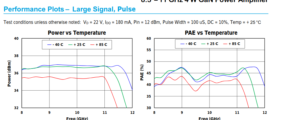
This is a GaN part. Applying a voltage to the drain whilst the gate is off will result in part failure. Therefore, if you pulse the gate then the pulse needs to be Vlow < Vth (cut-off voltage) and Vhigh equal to the gate voltage needed for the desired quiescent drain current.
Specs in the data sheet are exclusive to pulsed drain voltage. 100us pulse width at 10% duty cycle means that the drain voltage is on for 100us, 10% of the time. Remaining 90%, the drain is off to help negate the effects of thermals. Typically, you would also pulse the RF source too, at a slightly shorter pulse width - to allow for the drain voltage to reach its steady state and then turn the RF pulse on and back off before the drain voltage pulse turns off.
Pulsing the drain does have an advantage over pulsing the gate, although it is typically more difficult to achieve due to higher voltages/currents. Pulsing the drain is preferred as it results in faster rise times, and in turn, shorter allowable pulse widths. This is due to the total input capacitance (derived from Qg, (where Q = C*V), not Ciss) having an impact of the rise time of the pulse, as the gate capacitance needs to charge up before the device can begin to conduct any current (turn on). Slower rise times directly impacts the minimum allowable pulse width.


