2
\$\begingroup\$

I am laying out an ADuM260N digital isolator. There is some higher frequency switching (~20MHz) on other components also connected to the input (left) voltage rail. I read this thread on decoupling, but there doesn't seem to be any consensus on the best via layout, specifically whether to connect the vias to the IC pin or the capacitor pin.

After reading the grounding sections of Ott's Electromagnetic Compatibility Engineering, two takeaways are:

  • Add multiple vias to power/ground to reduce loop inductance
  • Reduce mutual inductance by spacing out vias carrying current in the same direction (eg. GND and GND), and by moving vias closer that carry current in opposite directions (eg. PWR and GND)

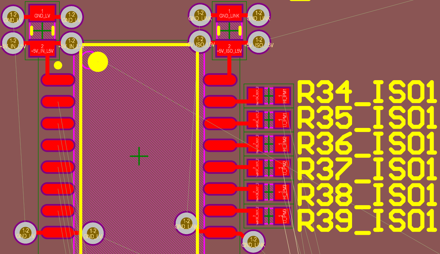
From these takeaways, my attempted layout is below:

enter image description here

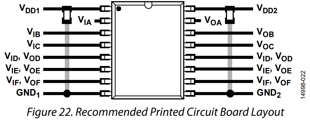
This is the datasheet's recommended layout:

enter image description here

From this, I have a few questions:

  1. Should I be connecting the vias of the 5V nets to the IC pin or to the capacitor pin?
  2. Could using two vias per net in this way somehow harm EMI/EMC performance?
  3. Is the datasheet recommendation of connecting the decoupling capacitor GND across the IC directly to the GND pin of the IC, a good idea?

Thanks!

\$\endgroup\$
2
  • 1
    \$\begingroup\$ How many layers is this PCB? What is your stack up? Do you have a GND pour? \$\endgroup\$
    – Puffafish
    Commented Aug 25, 2020 at 7:47
  • \$\begingroup\$ This will be a 6-8 layer PCB with both PWR and GND planes connected directly to their respective vias \$\endgroup\$
    – w00t
    Commented Aug 25, 2020 at 8:12

2 Answers 2

5
\$\begingroup\$

Looking at EMC is important. Placement of decoupling capacitors is important, and placement of vias can be more important. Well done for considering it.

The general rule is: make the inductive loop as small as possible.

Assuming you have a 4 layer PCB, the middle two layers are a GND plane and a power plane. This means that you can then put a via at the IC power pins, and at the IC GND pins, so that power and GND are both connected straight to the plane.

You can then also connect the capacitors GND and power pins straight to vias. This way you can put the capacitors in the most sensible place between the GND and POWER of the IC depending on the other restrictions on your board.

As mentioned by yourself; you want to reduce the inductive loop between power and ground with the capacitors. This is reducing the loop for the IC (the thing you're decoupling), and so ideally you want the capacitors rotated by 90 compared to how you have them, as that reduces the loop by the size of the capacitor. There is an argument that this will make a small difference, as the parasitic inductance in the capacitor is probably going to have more of an impact. But every little helps! (Using the physically smallest capacitors as possibly will help too).

To directly answer your questions:

  1. Connect the vias to both the IC and the capacitors
  2. The more vias to connect to power and ground is sometimes better, rarely worse
  3. The datasheet is showing how to reduce the inductive loop between the power and ground pin of the IC (by connecting them as tightly as possible) so that is a good idea.
\$\endgroup\$
4
  • 1
    \$\begingroup\$ Thank you for the detailed response! To clarify, connecting the vias directly to the IC refers to this type of layout: imgur.com/a/2VYRT19. Would a better via layout for the +5V rails look like this - imgur.com/a/mmYjVXU? This would have the least mutual inductance between vias, and the shortest ground loop for both the IC and the decoupling cap. \$\endgroup\$
    – w00t
    Commented Aug 25, 2020 at 8:12
  • 1
    \$\begingroup\$ @w00t The first picture would be fine, but the capacitor could be moved closer in to reduce the inductive loop more. The second picture would also be ok, but the capacitor could be rotated to reduce the loop again. \$\endgroup\$
    – Puffafish
    Commented Aug 25, 2020 at 8:14
  • 1
    \$\begingroup\$ @w00t, I agree with everything in this answer. That said, at 20 MHz, with ~9 mm between the power and ground pins of the chip, you don't need to worry about 0.01's of mm difference in the placement of your capacitor. \$\endgroup\$
    – The Photon
    Commented Aug 25, 2020 at 15:05
  • \$\begingroup\$ Ah, I now see how rotating the capacitor 90 degrees reduces the inductive loop. Might as well do it anyways to conserve space. Thank you both! \$\endgroup\$
    – w00t
    Commented Aug 25, 2020 at 18:24
2
\$\begingroup\$

This IC package will have a LARGE internal metal leadframe.

You can greatly reduce the "enclosed-loop-area" by placing the bypass cap

UNDER

the IC on backside of the PCB.

Imagine the cap is under the center of he IC, with PCB traces running away from the cap to the upper left IC solder pad, and running away from the other cap terminal to the lower left IC solder pad.

These PCB traces will be immediately UNDER the metal structure hidden inside the black epoxy, and the energy_storage loop_area will be greatly reduced, which speeds up the rate of supplying charge into the IC.

================================================

Page 21 of the datasheet has LINK to AppNote. I'd use the layout they suggest

\$\endgroup\$
2
  • 1
    \$\begingroup\$ To be clear, the left and right sides (and decoupling caps) are isolated from each other. Would placing the decoupling caps on the bottom still reduce the loop area? \$\endgroup\$
    – w00t
    Commented Aug 25, 2020 at 19:01
  • \$\begingroup\$ Wouldn't that spoil the decoupling? Because then the power and ground pins will connect to the power/ground planes first, then the decoupling capacitors after. \$\endgroup\$ Commented Oct 24, 2022 at 16:35

Your Answer

By clicking “Post Your Answer”, you agree to our terms of service and acknowledge you have read our privacy policy.

Not the answer you're looking for? Browse other questions tagged or ask your own question.